ZHCSGK1 July 2017 TPS54424
PRODUCTION DATA.
- 1 特性
- 2 应用
- 3 说明
- 4 修订历史记录
- 5 Pin Configuration and Functions
- 6 Specifications
-
7 Detailed Description
- 7.1 Overview
- 7.2 Functional Block Diagram
- 7.3
Feature Description
- 7.3.1 Fixed Frequency PWM Control
- 7.3.2 Continuous Conduction Mode Operation (CCM)
- 7.3.3 VIN Pins and VIN UVLO
- 7.3.4 Voltage Reference and Adjusting the Output Voltage
- 7.3.5 Error Amplifier
- 7.3.6 Enable and Adjustable UVLO
- 7.3.7 Soft Start and Tracking
- 7.3.8 Safe Start-up into Pre-Biased Outputs
- 7.3.9 Power Good
- 7.3.10 Sequencing (SS/TRK)
- 7.3.11 Adjustable Switching Frequency (RT Mode)
- 7.3.12 Synchronization (CLK Mode)
- 7.3.13 Bootstrap Voltage and 100% Duty Cycle Operation (BOOT)
- 7.3.14 Output Overvoltage Protection (OVP)
- 7.3.15 Overcurrent Protection
- 7.4 Device Functional Modes
-
8 Application and Implementation
- 8.1 Application Information
- 8.2
Typical Application
- 8.2.1 Design Requirements
- 8.2.2
Detailed Design Procedure
- 8.2.2.1 Custom Design With WEBENCH® Tools
- 8.2.2.2 Switching Frequency
- 8.2.2.3 Output Inductor Selection
- 8.2.2.4 Output Capacitor
- 8.2.2.5 Input Capacitor
- 8.2.2.6 Output Voltage Resistors Selection
- 8.2.2.7 Soft-start Capacitor Selection
- 8.2.2.8 Undervoltage Lockout Set Point
- 8.2.2.9 Bootstrap Capacitor Selection
- 8.2.2.10 PGOOD Pull-up Resistor
- 8.2.2.11 Compensation
- 8.2.3 Application Curves
- 9 Power Supply Recommendations
- 10Layout
- 11器件和文档支持
- 12机械、封装和可订购信息
8 Application and Implementation
NOTE
Information in the following applications sections is not part of the TI component specification, and TI does not warrant its accuracy or completeness. TI’s customers are responsible for determining suitability of components for their purposes. Customers should validate and test their design implementation to confirm system functionality.
8.1 Application Information
The TPS54424 is a synchronous buck converter designed for 4.5 V to 17 V input and 4-A load. This procedure illustrates the design of a high-frequency switching regulator using ceramic output capacitors. Alternatively the WEBENCH® software can be used to generate a complete design. The WEBENCH® software uses an interactive design procedure and accesses a comprehensive database of components when generating a design. This section presents a simplified discussion of the design process.
8.2 Typical Application
8.2.1 Design Requirements
For this design example, use the parameters shown in Table 1.
Table 1. Design Parameters
| PARAMETER | EXAMPLE VALUE |
|---|---|
| Input voltage range (VIN) | 4.5 to 15 V, 12 V Nominal |
| Output voltage (VOUT) | 1.8 V |
| Transient response | +/- 4%, +/- 72 mV |
| Output ripple voltage | 0.5%, 9 mV |
| Output current rating (IOUT) | 4 A |
| Operating frequency (fSW) | 700 kHz |
8.2.2 Detailed Design Procedure
8.2.2.1 Custom Design With WEBENCH® Tools
Click here to create a custom design using the TPS54424 device with the WEBENCH® Power Designer.
- Start by entering the input voltage (VIN), output voltage (VOUT), and output current (IOUT) requirements.
- Optimize the design for key parameters such as efficiency, footprint, and cost using the optimizer dial.
- Compare the generated design with other possible solutions from Texas Instruments.
The WEBENCH Power Designer provides a customized schematic along with a list of materials with real-time pricing and component availability.
In most cases, these actions are available:
- Run electrical simulations to see important waveforms and circuit performance
- Run thermal simulations to understand board thermal performance
- Export customized schematic and layout into popular CAD formats
- Print PDF reports for the design, and share the design with colleagues
Get more information about WEBENCH tools at www.ti.com/WEBENCH.
8.2.2.2 Switching Frequency
The first step is to decide on a switching frequency for the converter. It is capable of running from 200 kHz to 1.6 MHz. Typically the highest switching frequency possible is desired because it will produce the smallest solution size. A high switching frequency allows for lower valued inductors and smaller output capacitors compared to a power supply that switches at a lower frequency. The main trade off made with selecting a higher switching frequency is extra switching power loss, which hurt the converter’s efficiency.
The maximum switching frequency for a given application is limited by the minimum on-time of the converter and is estimated with Equation 12. Using a maximum minimum on-time of 130 ns for the TPS54424 and 17 V maximum input voltage for this application, the maximum switching frequency is 814 kHz. Considering the 10% tolerance of the switching frequency, a switching frequency of 700 kHz was selected. Equation 13 calculates R7 to be 69.7 kΩ. A standard 1% 69.8 kΩ value was chosen in the design.

vertical spacer

8.2.2.3 Output Inductor Selection
To calculate the value of the output inductor, use Equation 14. KIND is a ratio that represents the amount of inductor ripple current relative to the maximum output current. The inductor ripple current is filtered by the output capacitor. Therefore, choosing high inductor ripple currents impacts the selection of the output capacitor since the output capacitor must have a ripple current rating equal to or greater than the inductor ripple current. Additionally with current mode control the sensed inductor current ripple is used in the PWM modulator. Choosing small inductor ripple currents can degrade the transient response performance or introduce jitter in the high-side MOSFET on-time. The inductor ripple, KIND, is normally from 0.2 to 0.4 for the majority of applications giving a peak to peak ripple current range of 0.8 A to 1.6 A. For applications requiring operation near the minimum on-time, with on-times less than 200 ns, the target Iripple must be 1.2 A or larger for best performance. For other applications the target Iripple should be 0.8 A or larger.
For this design example, KIND = 0.3 is used and the inductor value is calculated to be 1.92 μH. The nearest standard value 1.8 µH is selected. It is important that the RMS current and saturation current ratings of the inductor not be exceeded. The RMS and peak inductor current can be found from Equation 16 and Equation 17. For this design, the RMS inductor current is 4.0 A and the peak inductor current is 4.6 A. The chosen inductor is a Würth Elektronik 74438357018. It has a saturation current rating of 8.0 A (20% inductance loss) and a RMS current rating of 5.8 A (40 °C temperature rise). The DC series resistance is 18 mΩ typical.
The current flowing through the inductor is the inductor ripple current plus the output current. During power up, faults or transient load conditions, the inductor current can increase above the calculated peak inductor current level calculated in Equation 17. In transient conditions, the inductor current can increase up to the switch current limit of the device. For this reason, the most conservative approach is to specify the ratings of the inductor based on the switch current limit rather than the steady-state peak inductor current.

vertical spacer

vertical spacer

vertical spacer

8.2.2.4 Output Capacitor
There are two primary considerations for selecting the value of the output capacitor. The output voltage ripple and how the regulator responds to a large change in load current. The output capacitance needs to be selected based on the more stringent of these two criteria.
The desired response to a large change in the load current is the first criteria and is typically the most stringent. A regulator does not respond immediately to a large, fast increase or decrease in load current. The output capacitor supplies or absorbs charge until the regulator responds to the load step. The control loop needs to sense the change in the output voltage then adjust the peak switch current in response to the change in load. The minimum output capacitance is selected based on an estimate of the loop bandwidth. Typically the loop bandwidth is fSW/10. Equation 18 estimates the minimum output capacitance necessary, where ΔIOUT is the change in output current and ΔVOUT is the allowable change in the output voltage.
For this example, the transient load response is specified as a 4% change in VOUT for a load step of 2 A. Therefore, ΔIOUT is 2 A and ΔVOUT is 72 mV. Using these numbers gives a minimum capacitance of 63 μF. This value does not take the ESR of the output capacitor into account in the output voltage change. For ceramic capacitors, the effect of the ESR can be small enough to be ignored. Aluminum electrolytic and tantalum capacitors have higher ESR that must be considered for load step response.
Equation 19 calculates the minimum output capacitance needed to meet the output voltage ripple specification. Where fsw is the switching frequency, Vripple is the maximum allowable output voltage ripple, and Iripple is the inductor ripple current. In this case, the target maximum output voltage ripple is 9 mV. Under this requirement, Equation 19 yields 25 μF.
vertical spacer

vertical spacer

Where:
- ΔIOUT is the change in output current
- ΔVOUT is the allowable change in the output voltage
- fsw is the regulators switching frequency
vertical spacer
Equation 20 calculates the maximum combined ESR the output capacitors can have to meet the output voltage ripple specification and this shows the ESR should be less than 7 mΩ. In this case ceramic capacitors will be used and the ESR of ceramic capacitors is typically much less than 7 mΩ. Capacitors also have limits to the amount of ripple current they can handle without producing excess heat and failing. An output capacitor that can support the inductor ripple current must be specified. Capacitor datasheets specify the RMS (Root Mean Square) value of the maximum ripple current. Equation 21 can be used to calculate the RMS ripple current the output capacitor needs to support. For this application, Equation 21 yields 370 mA and the ceramic capacitors used in this design will have a ripple current rating much higher than this.

vertical spacer

X5R and X7R ceramic dielectrics or similar should be selected for power regulator capacitors because they have a high capacitance to volume ratio and are fairly stable over temperature. The output capacitor must also be selected with the DC bias and AC voltage derating taken into account. The derated capacitance value of a ceramic capacitor due to DC voltage bias and AC RMS voltage is usually found on the manufacturer's website. For this application example, one 100 μF 6.3 V 1210 X5R ceramic capacitor with 2 mΩ of ESR is used. The estimated capacitance after derating using the capacitor manufacturer's website is 80 µF.
8.2.2.5 Input Capacitor
The TPS54424 requires input decoupling ceramic capacitors type X5R, X7R or similar from VIN to PGND placed as close as possible to the IC. A total of at least 4.7 μF of capacitance is required and some applications may require a bulk capacitance. At least 1 µF of bypass capacitance is recommended near both VIN pins to minimize the input voltage ripple. A 0.1 µF to 1 µF capacitor must be placed by both VIN pins 2 and 11 to provide high frequency bypass to reduce the high frequency overshoot and ringing on VIN and SW pins. The voltage rating of the input capacitor must be greater than the maximum input voltage. The capacitor must also have a ripple current rating greater than the maximum RMS input current of the TPS54424. The RMS input current can be calculated using Equation 22.
For this example design, a ceramic capacitor with at least a 25 V voltage rating is required to support the maximum input voltage. Two 10 µF 1206 X5R 25 V and two 0.1 μF 0603 X7R 25 V capacitors in parallel has been selected to be placed on both sides of the IC near both VIN pins to PGND pins. Based on the capacitor manufacturer's website, the total ceramic input capacitance derates to 7.6 µF at the nominal input voltage of 12 V. A 100 µF bulk capacitance is also used in this circuit to bypass long leads when connected a lab bench top power supply.
The input capacitance value determines the input ripple voltage of the regulator. The input voltage ripple can be calculated using Equation 23. The maximum input ripple occurs when operating nearest to 50% duty cycle. Using the nominal design example values of Ioutmax = 4 A, Cin = 7.6 μF, and fSW = 700 kHz, the input voltage ripple with the 12 V nominal input is 100 mV and the RMS input ripple current with the 4.5 V minimum input is 2.0 A.

vertical spacer

8.2.2.6 Output Voltage Resistors Selection
The output voltage is set with a resistor divider created by R8 (RFBT) and R6 (RFBB) from the output node to the FB pin. It is recommended to use 1% tolerance or better resistors. For this example design, 6.04 kΩ was selected for R8. Using Equation 24, R6 is calculated as 12.08 kΩ. The nearest standard 1% resistor is 12.1 kΩ.

8.2.2.7 Soft-start Capacitor Selection
The soft-start capacitor determines the amount of time it takes for the output voltage to reach its nominal programmed value during power up. This is useful if a load requires a controlled voltage slew rate. This is also used if the output capacitance is very large and would require large amounts of current to quickly charge the capacitor to the output voltage level. The large currents necessary to charge the capacitor may make the TPS54424 reach its current limit or cause the input voltage rail to sag due excessive current draw from the input power supply. Limiting the output voltage slew rate solves both of these problems. The soft-start capacitor value can be calculated using Equation 25. For the example circuit, the soft-start time is not critical because the output capacitor value of 100 μF does not require much current to charge to 1.8 V. The example circuit has the soft-start time set to an arbitrary value of 1 ms which requires a 8.2-nF capacitor.

8.2.2.8 Undervoltage Lockout Set Point
The Undervoltage Lockout (UVLO) is adjusted using the external voltage divider network of R2 (RENT) and R9 (RENB). The UVLO has two thresholds; one for power up when the input voltage is rising and one for power-down or brown outs when the input voltage is falling. For the example design, the supply should turn on and start switching once the input voltage increases above 4.5 V (UVLO start or enable). After the regulator starts switching, it should continue to do so until the input voltage falls below 4.0 V (UVLO stop or disable). Equation 2 and Equation 3 can be used to calculate the values for the upper and lower resistor values. For the voltages specified, the standard resistor value used for R2 is 86.6 kΩ and for R4 is 30.9 kΩ.
8.2.2.9 Bootstrap Capacitor Selection
A 0.1-µF ceramic capacitor must be connected between the BOOT to SW pin for proper operation. A 1 Ω to 5.6 Ω resistor can be added in series with the BOOT capacitor to slow down the turn on of the high-side MOSFET. This can reduce voltage spikes on the SW node with the trade off of more power loss and lower efficiency.
8.2.2.10 PGOOD Pull-up Resistor
A 100 kΩ resistor is used to pull-up the power good signal when FB conditions are met. The pull-up voltage source must be less than the 6.5 V absolute maximum of the PGOOD pin.
8.2.2.11 Compensation
There are several methods used to compensate DC - DC regulators. The method presented here is easy to calculate and ignores the effects of the slope compensation internal to the device. Because the slope compensation is ignored, the actual cross-over frequency will usually be lower than the cross-over frequency used in the calculations. This method assumes the cross-over frequency is between the modulator pole and the ESR zero and the ESR zero is at least 10 times greater the modulator pole. This is the case when using low ESR output capacitors. Use the WEBENCH® software for more accurate loop compensation. These tools include a more comprehensive model of the control loop.
To get started, the modulator pole, fpmod, and the ESR zero, fz1 must be calculated using Equation 26 and Equation 27. For Cout, use a derated value of 80 μF and an ESR of 2 mΩ. Use equations Equation 28 and Equation 29, to estimate a starting point for the crossover frequency, fco, to design the compensation. For the example design, fpmod is 4.4 kHz and fzmod is 995 kHz. Equation 28 is the geometric mean of the modulator pole and the ESR zero. Equation 29 is the mean of modulator pole and one half the switching frequency. Equation 28 yields 66 kHz and Equation 29 gives 39 kHz. Use the lower value of Equation 28 or Equation 29 for an initial crossover frequency. Next, the compensation components are calculated. A resistor in series with a capacitor is used to create a compensating zero. A capacitor in parallel to these two components forms the compensating pole.

vertical spacer

vertical spacer

vertical spacer

To determine the compensation resistor, R5, use Equation 30. R5 is calculated to be 3.17 kΩ and the closest standard value 3.16 kΩ. Use Equation 31 to set the compensation zero to the modulator pole frequency. Equation 31 yields 11.4 nF for compensating capacitor C18 and the closest standard value is 0.012 µF.

Where:
- Power stage transconductance, gmPS = 17 A/V
- VOUT = 1.8 V
- VREF = 0.6 V
- Error amplifier transconductance, gmEA = 1100 µA/V

A compensation pole is implemented using an additional capacitor C17 in parallel with the series combination of R5 and C18. This capacitor is recommended to help filter any noise that may couple to the COMP voltage signal. Use the larger value of Equation 32 and Equation 33 to calculate the C17 and to set the compensation pole. C17 is calculated to be the largest of 41 pF and 134 pF. The closest standard value is 120 pF.

vertical spacer

Type III compensation can be used by adding the feed forward capacitor C19 in parallel with the upper feedback resistor. Type III compensation adds phase boost above what is possible from type II compensation because it places an additional zero/pole pair. The zero/pole pair is not independent. As a result once the zero location is chosen, the pole is fixed as well. The zero is placed at 1/2 the fSW by calculating the value of C19 with Equation 34. The calculated value is 37 pF and the closest standard value is 39 pF. It is possible to use larger feedforward capacitors to further improve the transient response but care should be taken to ensure there is a minimum of -10 dB gain margin at 1/2 the fSW in all operating conditions. The feedforward capacitor injects noise on the output into the FB pin and this added noise can result in more jitter at the switching node. To little gain margin can cause a repeated wide and narrow pulse behavior. This example design does not use the optional feedforward capacitor.

The initial compensation based on these calculations is R5 = 3.16 kΩ, C18 = 0.012 µF, and C17 = 120 pF. These values yield a stable design but after testing the real circuit these values were changed to target a higher crossover frequency to improve transient response performance. The crossover frequency is increased by increasing the value of R5 and decreasing the value of the compensation capacitors. The final values used in this example are R5 = 3.48 kΩ, C18 = 8200 pF, and C17 = 68 pF.
8.2.3 Application Curves
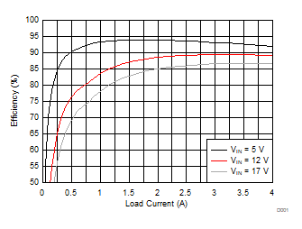
| TA = 25°C | VOUT = 1.8 V | fSW = 700 kHz |
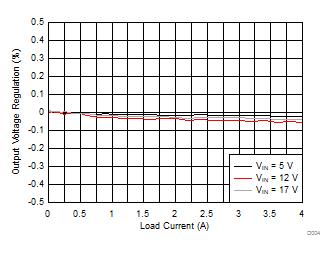
| TA = 25°C | VOUT = 1.8 V | fSW = 700 kHz |
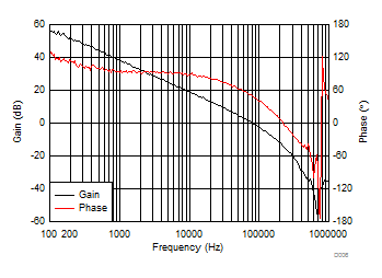
| VIN = 12 V | VOUT = 1.8 V | IOUT = 2 A |
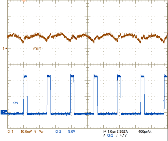
| VIN = 12 V | VOUT = 1.8 V | IOUT = 0 A |
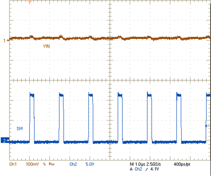
| VIN = 12 V | VOUT = 1.8 V | IOUT = 0 A |
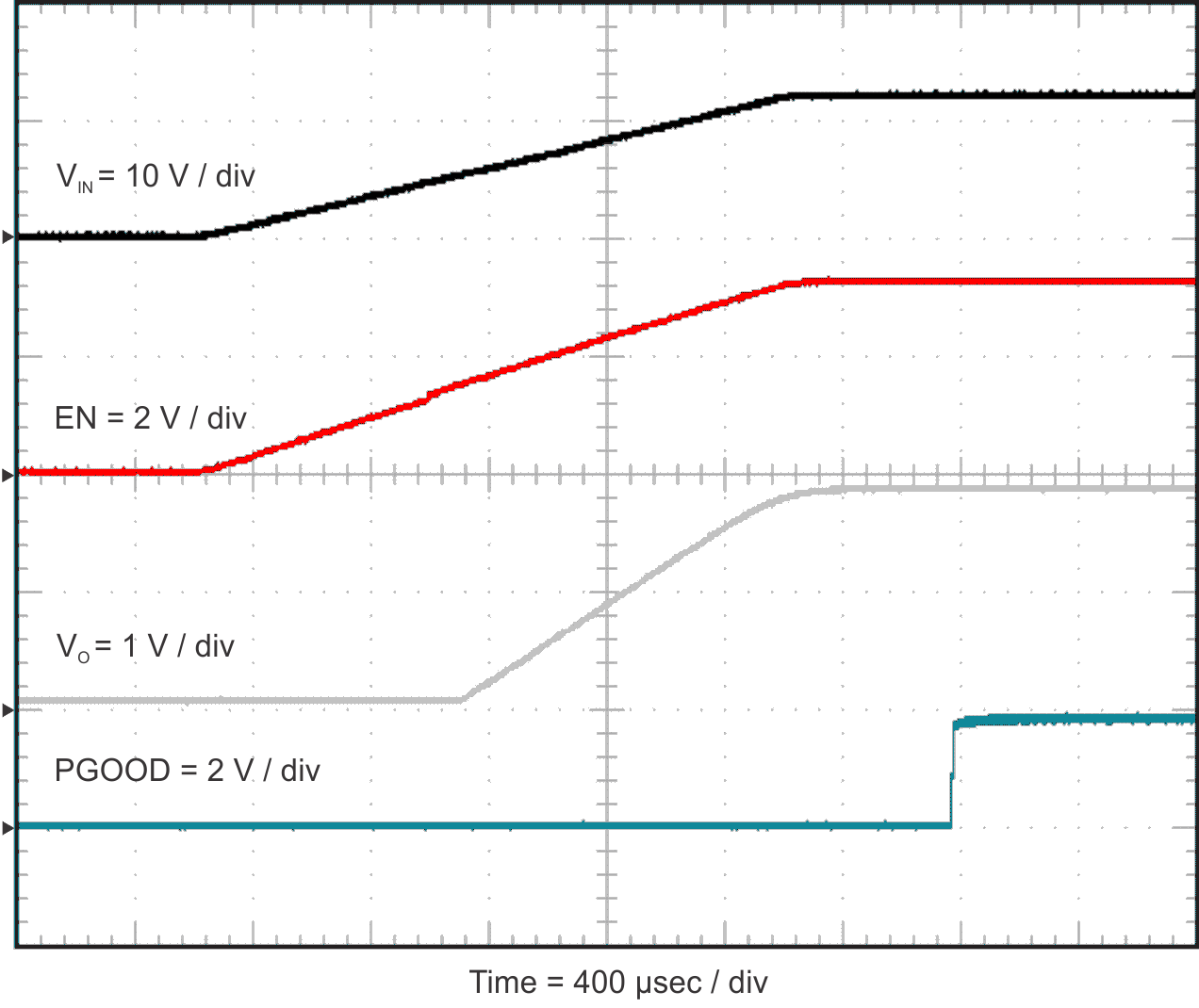
| RLOAD = 1 Ω |
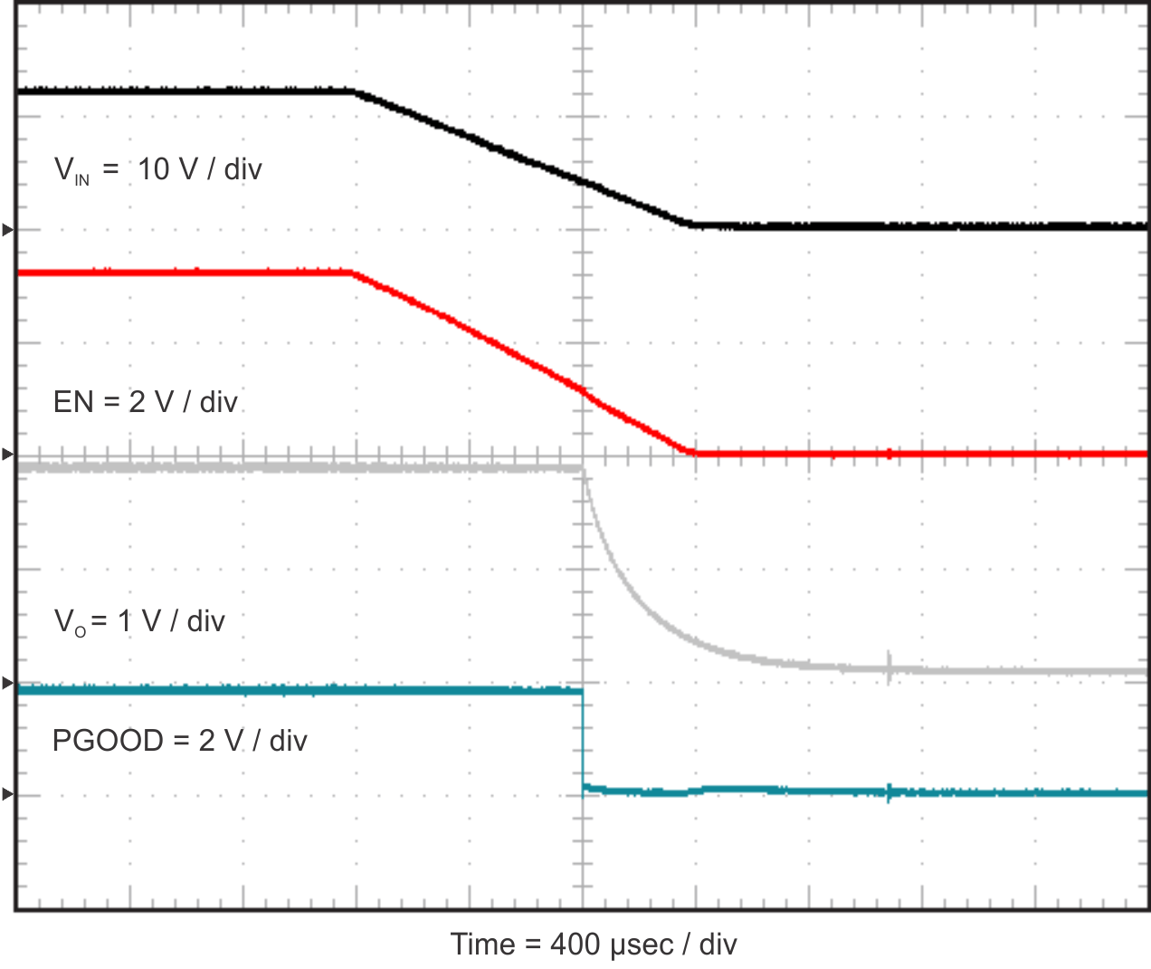
| RLOAD = 1 Ω | VIN = 12 V |
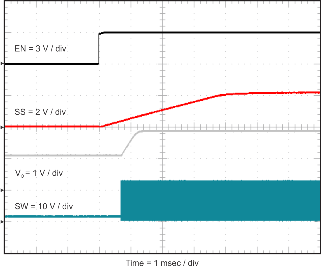
| VIN = 12 V |
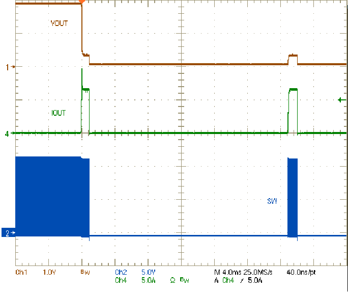
| VIN = 12 V | IOUT = short |
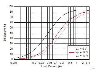
| TA = 25°C | VOUT = 1.8 V | fSW = 700 kHz |
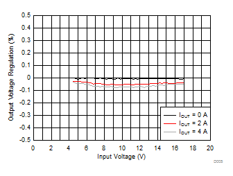
| TA = 25°C | VOUT = 1.8 V | fSW = 700 kHz |
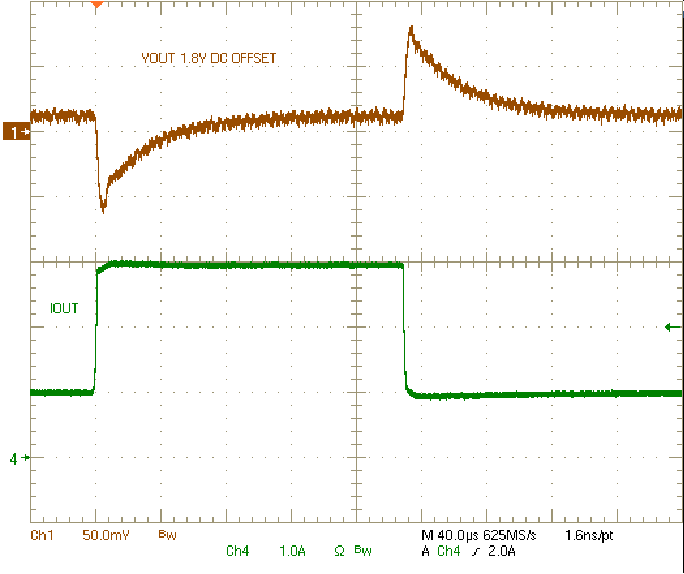
| VIN = 12 V | VOUT = 1.8 V |
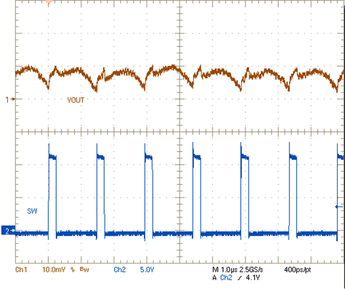
| VIN = 12 V | VOUT = 1.8 V | IOUT = 4 A |
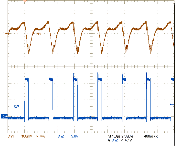
| VIN = 12 V | VOUT = 1.8 V | IOUT = 4 A |
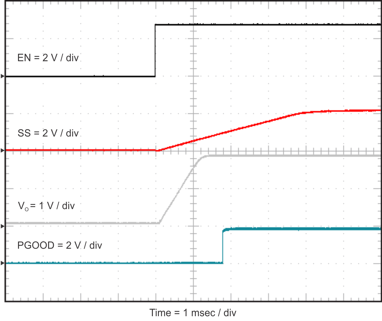
| RLOAD = 1 Ω |
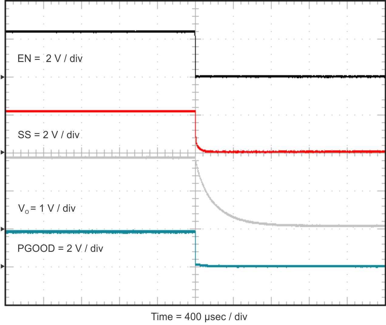
| RLOAD = 1 Ω |
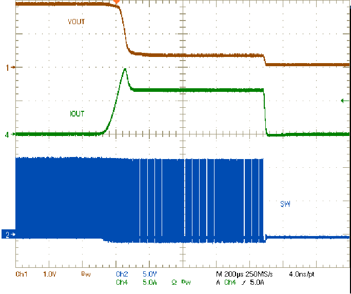
| VIN = 12 V | IOUT = short |
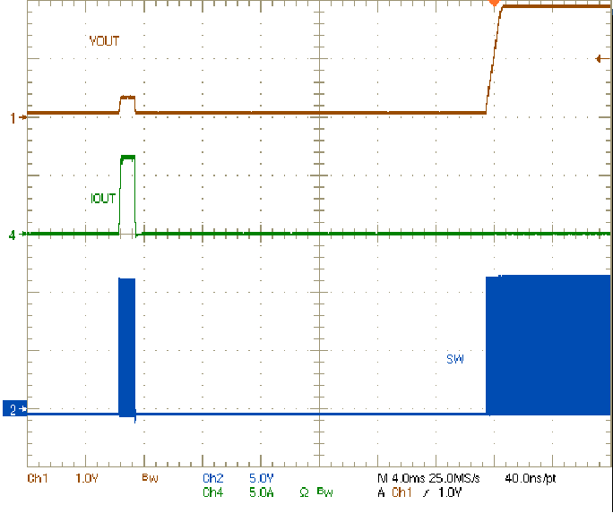
| VIN = 12 V | IOUT = short removed |