SLUSCJ3A April 2016 – June 2016 TPS53632G
PRODUCTION DATA.
- 1 Features
- 2 Applications
- 3 Description
- 4 Revision History
- 5 Pin Configuration and Functions
- 6 Specifications
- 7 Timing Requirements
- 8 Switching Characteristics
- 9 Typical Characteristics (Half-Bridge Operation)
-
10Detailed Description
- 10.1 Overview
- 10.2 Functional Block Diagram
- 10.3
Feature Description
- 10.3.1 Current Sensing
- 10.3.2 Load Transients
- 10.3.3 PWM and SKIP Signals
- 10.3.4 5-V, 3.3-V and 1.8-V Undervoltage Lockout (UVLO)
- 10.3.5 Output Undervoltage Protection (UVP)
- 10.3.6 Overcurrent Protection (OCP)
- 10.3.7 Overvoltage Protection
- 10.3.8 Analog Current Monitor, IMON and Corresponding Digital Output Current
- 10.3.9 Addressing
- 10.3.10 I2C Interface Operation
- 10.3.11 Start-Up Sequence
- 10.3.12 Power Good Operation
- 10.3.13 Fault Behavior
- 10.4 Device Functional Modes
- 10.5 Configuration and Programming
- 10.6 Register Maps
-
11Applications and Implementation
- 11.1 Application Information
- 11.2
Typical Application
- 11.2.1
D-CAP+™ Half-Bridge Application
- 11.2.1.1 Design Requirements
- 11.2.1.2
Detailed Design Procedure
- 11.2.1.2.1 Step 1: Select Switching Frequency
- 11.2.1.2.2 Step 2: Set The Slew Rate
- 11.2.1.2.3 Step 3: Determine Inductor Value And Choose Inductor
- 11.2.1.2.4 Step 4: Determine Current Sensing Method
- 11.2.1.2.5 Step 5: DCR Current Sensing
- 11.2.1.2.6 Step 6: Select OCP Level
- 11.2.1.2.7 Step 7: Set the Load-Line Slope
- 11.2.1.2.8 Step 8: Current Monitor (IMON) Setting
- 11.2.1.3 Application Performance Plots
- 11.2.1.4 Loop Compensation for Zero Load-Line
- 11.2.1
D-CAP+™ Half-Bridge Application
- 12Power Supply Recommendations
- 13 Layout
- 14Device and Documentation Support
- 15Mechanical, Packaging, and Orderable Information
13 Layout
13.1 Layout Guidelines
13.1.1 PCB Layout
- Check the pinout of the controller on schematic against the pinout of the datasheet.
- Have a component value calculator tool ready to check component values.
- Carefully check the choice of inductor and DCR.
- Carefully check the choice of output capacitors.
- Because the voltage and current feedback signals are fully differential, double check their polarity.
- CSP1 / CSN1
- CSP2 / CSN2
- VOUT_SENSE to VFB / GND_SENSE to GFB
- Make sure the pull-up on the SDA, and SCL lines are correct. Ensure there is a bypass capacitor close to the device on the pull-up VINTF rail to GND of the device.
- TI strongly recommends that the device GND be separate from the system and Power GND.
MOST CRITICAL LAYOUT RULE
Make sure to separate noisy driver interface lines.
The driver is outside of the device. All gate-drive and switch-node traces must be local to the inductor and MOSFETs.
13.1.2 Current Sensing Lines
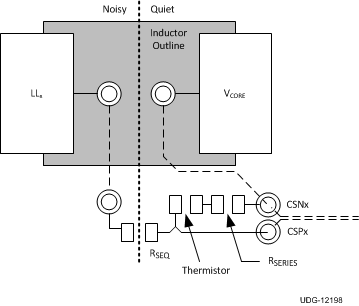
Given the physical layout of most systems, the current feedback (CSPx and CSNx) may have to pass near the power chain.
 Figure 20. Kelvin Connections To The Inductor For DCR Sensing
Good load-line, current sharing, and current limiting performance of the TPS53632G device requires clean current feedback, so take the following precautions:
- Ensure all vias in the CSPx and CSNx traces are isolated from all other signals.
- TI recommends dotted signal traces be run in internal planes.
- If possible, change the name of the CSNx trace if possible to prevent automatic ties to the VCORE plane.
- Put RSEQU at the boundary between noisy and quiet areas.
- Run CSPx and CSNx as a differential pair in a quiet layer.
- Place the capacitor as near to the device pins as possible.
- Make a Kelvin connection to the pads of the resistor or inductor used for current sensing. See Figure 20 for a layout example.
- Run the current feedback signals as a differential pair to the device.
- Run the lines in a quiet layer. Isolate the lines from noisy signals by a voltage or ground plane.
- Put the compensation capacitor for DCR sensing (CSENSE) as close to the CS pins as possible.
- Place any noise filtering capacitors directly under or near the TPS53632G device and connect to the CS pins with the shortest trace length possible.
13.1.3 Feedback Voltage Sensing Lines
The voltage feedback coming from the CPU socket must be routed as a differential pair all the way to the VFB and GFB pins of the TPS53632G device. Avoid routing over switch-node and gate-drive traces.
13.1.4 PWM And SKIP Lines
The PWM and SKIP lines should be routed from the TPS53632G device to the driver without crossing any switch-node or the gate drive signals.
13.1.4.1 Minimize High Current Loops
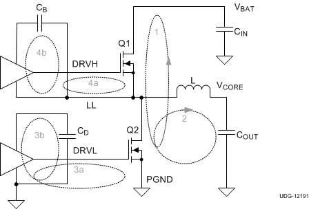
Figure 21 shows the primary current loops in each phase, numbered in order of importance.
 Figure 21. Major Current Loops To Minimize
The most important loop to minimize the area of is loop 1, the path from the input capacitor through the high and low-side FETs, and back to the capacitor through ground.
Loop 2 is from the inductor through the output capacitor, ground, and Q2. The layout of the low-side gate drive (Loops 3a and 3b) is important. The guidelines for the gate drive layout are:
- Make the low-side gate drive as short as possible (1 in or less preferred).
- Make the DRVL width to length ratio of 1:10, wider (1:5) if possible.
- If changing layers is necessary, use at least two vias.
13.1.5 Power Chain Symmetry
The TPS53632G device does not require special care in the layout of the power chain components because independent isolated current feedback is provided. Lay out the phases in a symmetrical manner, if possible. The rule is: the current feedback from each phase needs to be clean of noise and have the same effective current-sense resistance.
13.1.6 Component Location
Place components as close to the device in the following order.
- CS pin noise filtering components
- COMP pin and DROOP pin compensation components
- Decoupling capacitors for VREF, VDD, V5A, and VINTF
- Decoupling capacitor for VINTF rail, which is pullup voltage for the digital lines. This decoupling should be placed near the device to have good signal integrity.
- OCP-I resistors, FREQ_P resistors, SLEWA resistors, and RAMP resistors
13.1.7 Grounding Recommendations
The TPS53632G device has an analog ground and a thermal pad. The usual procedure for connecting these is:
- Keep the analog GND of the device and the power GND of the power circuit separate. The device analog GND and the power circuit power GND can be connected at one single quiet point in the layout.
- The thermal pad does not have an electrical connection to device. But the thermal pad must be connected to GND pin (pin 29) of the device to give good ground shielding. Do not connect the thermal pad to system GND.
- Tie the thermal pad to a ground island with at least 4 vias. All the analog components can connect to this analog ground island.
- The analog ground can be connected to any quiet spot on the system ground. A quiet spot is defined as a spot where no power supply switching currents are likely to flow. Use a single point connection from analog ground to the system ground.
- Ensure that the low-side MOSFET source connection and the input decoupling capacitors have a sufficient number of vias.
13.1.8 Decoupling Recommendations
- Decouple V5A and VDD to GND with a ceramic capacitor (with a value of at least 1 µF) .
- Decouple VINTF to GND with a capacitor (with a value of at least 0.1 µF) to GND.
13.1.9 Conductor Widths
- Follow TI guidelines with respect to the voltage feedback and logic interface connection requirements.
- Maximize the widths of power, ground, and drive signal connections.
- For conductors in the power path, be sure there is adequate trace width for the amount of current flowing through the traces.
- Make sure there are sufficient vias for connections between layers. Use 1 via minimum per ampere of current.
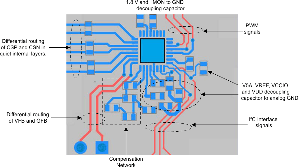
13.2 Layout Example
 Figure 22. Example Layout