ZHCSEM8 January 2016 TPS50601-SP
PRODUCTION DATA.
- 1 特性
- 2 应用
- 3 说明
- 4 修订历史记录
- 5 说明 (续)
- 6 Pin Configuration and Functions
- 7 Specifications
-
8 Detailed Description
- 8.1 Overview
- 8.2 Functional Block Diagram
- 8.3
Feature Description
- 8.3.1 VIN and Power VIN Pins (VIN and PVIN)
- 8.3.2 PVIN vs Frequency
- 8.3.3 Voltage Reference
- 8.3.4 Adjusting the Output Voltage
- 8.3.5 Maximum Duty Cycle Limit
- 8.3.6 PVIN vs Frequency
- 8.3.7 Safe Start-Up into Prebiased Outputs
- 8.3.8 Error Amplifier
- 8.3.9 Slope Compensation
- 8.3.10 Enable and Adjust UVLO
- 8.3.11 Adjustable Switching Frequency and Synchronization (SYNC)
- 8.3.12 Slow Start (SS/TR)
- 8.3.13 Power Good (PWRGD)
- 8.3.14 Bootstrap Voltage (BOOT) and Low Dropout Operation
- 8.3.15 Sequencing (SS/TR)
- 8.3.16 Output Overvoltage Protection (OVP)
- 8.3.17 Overcurrent Protection
- 8.3.18 TPS50601-SP Thermal Shutdown
- 8.3.19 Turn-On Behavior
- 8.3.20 Small Signal Model for Loop Response
- 8.3.21 Simple Small Signal Model for Peak Current Mode Control
- 8.3.22 Small Signal Model for Frequency Compensation
- 8.4 Device Functional Modes
-
9 Application and Implementation
- 9.1 Application Information
- 9.2
Typical Application
- 9.2.1 Design Requirements
- 9.2.2
Detailed Design Procedure
- 9.2.2.1 Operating Frequency
- 9.2.2.2 Output Inductor Selection
- 9.2.2.3 Output Capacitor Selection
- 9.2.2.4 Input Capacitor Selection
- 9.2.2.5 Slow Start Capacitor Selection
- 9.2.2.6 Bootstrap Capacitor Selection
- 9.2.2.7 Undervoltage Lockout (UVLO) Set Point
- 9.2.2.8 Output Voltage Feedback Resistor Selection
- 9.2.2.9 Compensation Component Selection
- 9.2.3 Application Curve
- 10Power Supply Recommendations
- 11Layout
- 12器件和文档支持
- 13机械、封装和可订购信息
8 Detailed Description
8.1 Overview
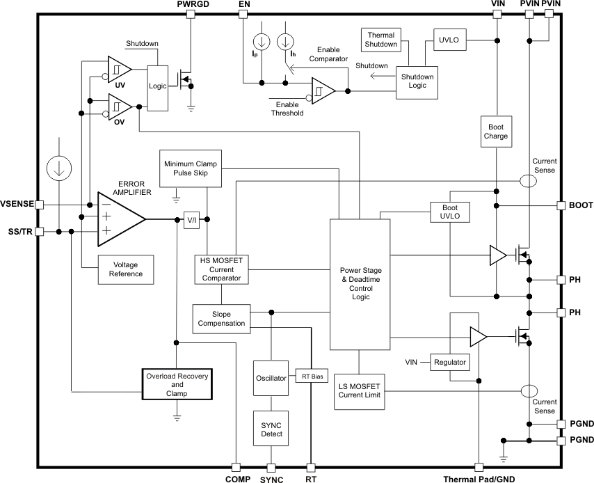
The device is a 6.3-V or 6-A synchronous step-down (buck) converter with two integrated N-channel MOSFETs. To improve performance during line and load transients, the device implements a constant frequency, peak current mode control, which also simplifies external frequency compensation. The wide switching frequency, 100 kHz to 1 MHz, allows for efficiency and size optimization when selecting the output filter components.
The device is designed for safe monotonic startup into prebiased loads. The default start up is when VIN is typically 3 V. The EN pin has an internal pullup current source that can be used to adjust the input voltage UVLO with two external resistors. In addition, the EN pin can be floating for the device to operate with the internal pullup current. The total operating current for the device is approximately 5 mA when not switching and under no load. When the device is disabled, the supply current is typically less than 2.5 mA.
The integrated MOSFETs allow for high-efficiency power supply designs with continuous output currents up to 6 A. The MOSFETs have been sized to optimize efficiency for lower duty cycle applications.
The device reduces the external component count by integrating the boot recharge circuit. The bias voltage for the integrated high-side MOSFET is supplied by a capacitor between the BOOT and PH pins. The boot capacitor voltage is monitored by a BOOT to PH UVLO (BOOT-PH UVLO) circuit allowing the PH pin to be pulled low to recharge the boot capacitor. The device can operate over duty cycle range per Equation 2 and Equation 3 as long as the boot capacitor voltage is higher than the preset BOOT-PH UVLO threshold, which is typically 2.2 V. The output voltage can be stepped down to as low as the 0.795-V voltage reference (Vref).
The device has a power good comparator (PWRGD) with hysteresis which monitors the output voltage through the VSENSE pin. The PWRGD pin is an open-drain MOSFET which is pulled low when the VSENSE pin voltage is less than 91% or greater than 109% of the reference voltage Vref and asserts high when the VSENSE pin voltage is 94% to 106% of the Vref.
The SS/TR (slow start/tracking) pin is used to minimize inrush currents or provide power-supply sequencing during power-up. A small-value capacitor or resistor divider should be coupled to the pin for slow start or critical power-supply sequencing requirements.
The device is protected from output overvoltage, overload, and thermal fault conditions. The device minimizes excessive output overvoltage transients by taking advantage of the overvoltage circuit power good comparator. When the overvoltage comparator is activated, the high-side MOSFET is turned off and prevented from turning on until the VSENSE pin voltage is lower than 106% of the Vref. The device implements both high-side MOSFET overload protection and bidirectional low-side MOSFET overload protections, which help control the inductor current and avoid current runaway. The device also shuts down if the junction temperature is higher than thermal shutdown trip point. The device is restarted under control of the slow-start circuit automatically when the junction temperature drops 10°C typical below the thermal shutdown trip point.
8.2 Functional Block Diagram
8.3 Feature Description
8.3.1 VIN and Power VIN Pins (VIN and PVIN)
The device allows for a variety of applications by using the VIN and PVIN pins together or separately. The VIN pin voltage supplies the internal control circuits of the device. The PVIN pin voltage provides the input voltage to the power converter system.
If tied together, the input voltage for VIN and PVIN can range from 3 to 6.3 V. If using the VIN separately from PVIN, the VIN pin must be between 3 and 6.3 V, and the PVIN pin can range from as low as 1.6 to 6.3 V. A voltage divider connected to the EN pin can adjust the input voltage UVLO appropriately. Adjusting the input voltage UVLO on the PVIN pin helps to provide consistent power-up behavior.
8.3.2 PVIN vs Frequency
With VIN tied to PVIN, minimum off-time determines what output voltage is achievable over frequency range.
8.3.3 Voltage Reference
The voltage reference system produces a precise voltage reference as indicated in Electrical Characteristics.
8.3.4 Adjusting the Output Voltage
The output voltage is set with a resistor divider from the output (VOUT) to the VSENSE pin. TI recommends to use 1% tolerance or better divider resistors. Start with a 10 kΩ for R15 (top resistor) and use Equation 1 to calculate R38 (bottom resistor divider). To improve efficiency at light loads, consider using larger-value resistors. If the values are too high, the regulator is more susceptible to noise and voltage errors from the VSENSE input current are noticeable.

where
- Vref = 0.795 V
The minimum output voltage and maximum output voltage can be limited by the minimum on-time of the high-side MOSFET and bootstrap voltage (BOOT-PH voltage) respectively. For more information, see Bootstrap Voltage (BOOT) and Low Dropout Operation.
8.3.5 Maximum Duty Cycle Limit
The TPS50601-SP can operate at duty cycle per Equation 2 and Equation 3 as long as the boot capacitor voltage is higher than the preset BOOT-PH UVLO threshold, which is typically 2.2 V.
Duty cycle can be calculated based on Equation 2.

where
- RTesr = Rdcr + Rtrace
- Rdcr is the dc resistance of the inductor.
- Rtrace is the dc trace resistance (miscellaneous drop).
- Rds_high is the maximum RDS of the high-side MOSFET.
- Rds_low is the maximum RDS of the low-side MOSFET.
8.3.6 PVIN vs Frequency
With VIN tied to PVIN, minimum off-time determines the output voltage that is achievable over frequency range. For VIN = PVIN must be ≥ 3 V. For VIN = 3 V, PVIN can vary from 1.6 to 6.3 V as highlighted in Electrical Characteristics.
This is given by Equation 3.

where
- Rds_onLS = Low-side Rds-on
- Rmisc = Miscellaneous trace drops
- Toff_min = Minimum off time
Using this approach, the designer can calculate minimum PVIN required for specific VOUT as indicated in the example in Figure 17.
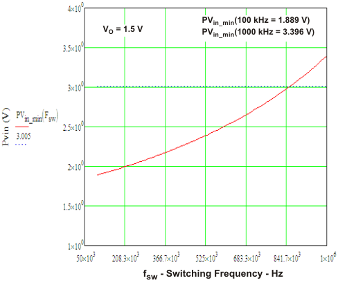 Figure 17. PVIN vs Frequency
8.3.7 Safe Start-Up into Prebiased Outputs
The device is designed to prevent the low-side MOSFET from discharging a prebiased output. During monotonic prebiased startup, the low-side MOSFET is not allowed to sink current until the SS/TR pin voltage is higher than 1.4 V.
8.3.8 Error Amplifier
The device uses a transconductance error amplifier. The error amplifier compares the VSENSE pin voltage to the lower of the SS/TR pin voltage or the internal 0.795-V voltage reference. The transconductance of the error amplifier is 1300 μA/V during normal operation. The frequency compensation network is connected between the COMP pin and ground. Error amplifier dc gain is typically 39000 V/V with minimum value of 22000 V/V per design.
8.3.9 Slope Compensation
The device adds a compensating ramp to the switch current signal. This slope compensation prevents subharmonic oscillations. The available peak inductor current remains constant over the full duty cycle range. Minimum peak-to-peak inductor current should be greater than 1 A.
8.3.10 Enable and Adjust UVLO
The EN pin provides electrical on and off control of the device. When the EN pin voltage exceeds the threshold voltage, the device starts operation. If the EN pin voltage is pulled below the threshold voltage, the regulator stops switching and enters low Iq state. If an external Schottky diode is used from VIN to boot, then a bleeder may be required <1 mA to ensure output is low when the unit is disabled by EN pin.
The EN pin has an internal pullup current source, allowing the user to float the EN pin for enabling the device. If an application requires controlling the EN pin, use open-drain or open-collector output logic to interface with the pin.
The device implements internal UVLO circuitry on the VIN pin. The device is disabled when the VIN pin voltage falls below the internal VIN UVLO threshold. The internal VIN UVLO threshold has a hysteresis of 50 mV typical.
If an application requires either a higher UVLO threshold on the VIN pin or a secondary UVLO on the PVIN in split-rail applications, then the EN pin can be configured as shown in Figure 18, Figure 19, and Figure 20. When using the external UVLO function, TI recommends to set the hysteresis to be >500 mV.
The EN pin has a small pullup current, Ip, which sets the default state of the pin to enable when no external components are connected. The pullup current is also used to control the voltage hysteresis for the UVLO function because it increases by Ih after the EN pin crosses the enable threshold. Calculate the UVLO thresholds with Equation 4 and Equation 5.
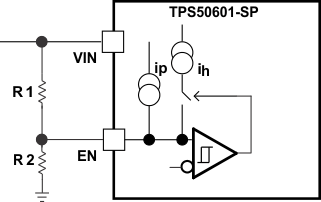 Figure 18. Adjustable VIN UVLO
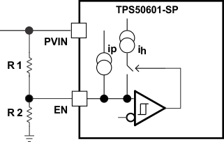 Figure 19. Adjustable PVIN UVLO, VIN ≥ 3 V
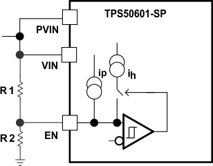 Figure 20. Adjustable VIN and PVIN UVLO
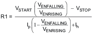

where
- Ih = 3 μA
- Ip = 3.2 μA
- VENRISING = 1.131 V
- VENFALLING = 1.09 V
8.3.11 Adjustable Switching Frequency and Synchronization (SYNC)
The switching frequency of the device supports three modes of operations. The modes of operation are set by the conditions on the RT and SYNC pins. At a high level, these modes can be described as master, internal oscillator, and external synchronization modes.
In master mode, the RT pin should be left floating; the internal oscillator is set to 500 kHz, and the SYNC pin is set as an output clock. The SYNC output is in phase with respect to the internal oscillator. SYNC out signal level is the same as VIN level with 50% duty cycle. SYNC signal feeding the slave module—which is in phase with the master clock—gets internally inverted (180° out of phase with the master clock) internally in the slave module.
In internal oscillator mode, a resistor is connected between the RT pin and GND. The SYNC pin requires a 10-kΩ resistor to GND for this mode to be effective. The switching frequency of the device is adjustable from 100 kHz to 1 MHz by placing a maximum of 510 kΩ and a minimum of 47 kΩ respectively. To determine the RT resistance for a given switching frequency, use Equation 6 or the curve in Figure 21. To reduce the solution size, the designer should set switching frequency as high as possible, but consider the tradeoffs of supply efficiency and minimum controllable on-time.

where
- RT in kΩ
- FSW in kHz
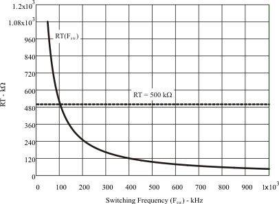 Figure 21. RT vs Switching Frequency
When operating the converter in internal oscillator mode (internal oscillator determines the switching frequency (500 kHz) default), the synchronous pin becomes the output and there is a phase inversion. When trying to parallel with another converter, the RT pin of the second (slave) converter must have its RT pin populated such that the converter frequency of the slave converter must be within ±5% of the master converter. This is required because the RT pin also sets the proper operation of slope compensation.
In external synchronization mode, a resistor is connected between the RT pin and GND. The Sync pin requires a toggling signal for this mode to be effective. The switching frequency of the device goes 1:1 with that of Sync pin. External system clock-user supplied sync clock signal determines the switching frequency. If no external clock signal is detected for 20 µs, then TPS50601-SP transitions to its internal clock, which is typically 500 kHz. An external synchronization using an inverter to obtain phase inversion is necessary. RT values of the master and slave converter must be within ±5% of the external synchronization frequency. This is necessary for proper slope compensation. A resistance in the RT pin is required for proper operation of the slope compensation circuit. To determine the RT resistance for a given switching frequency, use Equation 6 or the curve in Figure 21. To reduce the solution size, the designer should set switching frequency as high as possible, but consider the tradeoffs of supply efficiency and minimum controllable on-time.
These modes are described in Table 1.
Table 1. Switching Frequency, SYNC and RT Pin Usage Table
| RT PIN | SYNC PIN | SWITCHING FREQUENCY | DESCRIPTION AND NOTES |
|---|---|---|---|
| Float | Generates an output signal | 500 kHz | SYNC pin behaves as an output. SYNC output signal is 180° out of phase to the internal 500-kHz switching frequency. |
| 47- to 485-kΩ resistor to AGND | 10-kΩ resistor to AGND | 100 kHz to 1 MHz | Internally generated switching frequency is based upon the resistor value present at the RT pin. |
| User-supplied sync clock or TPS50601-SP master device sync output |
Internally synchronized to external clock | Set value of RT that corresponds to the externally supplied sync frequency. |
8.3.12 Slow Start (SS/TR)
The device uses the lower voltage of the internal voltage reference or the SS/TR pin voltage as the reference voltage and regulates the output accordingly. A capacitor on the SS/TR pin to ground implements a slow-start time. The device has an internal pullup current source of 5 mA that charges the external slow-start capacitor. Equation 7 shows the calculations for the slow-start time (Tss, 10% to 90%) and slow-start capacitor (Css). The voltage reference (Vref) is 0.795 V and the slow-start charge current (Iss) is 2.5 μA.

When the input UVLO is triggered, the EN pin is pulled below 1.032 V, or a thermal shutdown event occurs the device stops switching and enters low current operation. At the subsequent power-up, when the shutdown condition is removed, the device does not start switching until it has discharged its SS/TR pin to ground ensuring proper soft-start behavior.
8.3.13 Power Good (PWRGD)
The PWRGD pin is an open-drain output. When the VSENSE pin is between 94% and 106% of the internal voltage reference, the PWRGD pin pull-down is deasserted and the pin floats. TI recommends to use a pullup resistor between 10 to 100 kΩ to a voltage source that is 5.5 V or less. The PWRGD is in a defined state when the VIN input voltage is greater than 1 V but has reduced current sinking capability. The PWRGD achieves full current sinking capability when the VIN input voltage is above 3 V.
The PWRGD pin is pulled low when VSENSE is lower than 91% or greater than 109% of the nominal internal reference voltage. Also, the PWRGD is pulled low, if the input UVLO or thermal shutdown are asserted, the EN pin is pulled low or the SS/TR pin is below 1.4 V.
8.3.14 Bootstrap Voltage (BOOT) and Low Dropout Operation
The device has an integrated boot regulator, and requires a small ceramic capacitor between the BOOT and PH pins to provide the gate drive voltage for the high-side MOSFET. The boot capacitor is charged when the BOOT pin voltage is less than VIN and BOOT-PH voltage is below regulation. The value of this ceramic capacitor should be 0.1 μF. TI recommends a ceramic capacitor with an X7R- or X5R-grade dielectric with a voltage rating of 10 V or higher because of the stable characteristics over temperature and voltage.
To improve dropout, the device is designed to operate at a high duty cycle as long as the BOOT to PH pin voltage is greater than the BOOT-PH UVLO threshold, which is typically 2.1 V. When the voltage between BOOT and PH drops below the BOOT-PH UVLO threshold, the high-side MOSFET is turned off and the low-side MOSFET is turned on allowing the boot capacitor to be recharged. In applications with split-input voltage rails, high duty cycle operation can be achieved as long as (VIN – PVIN) > 4 V.
Maximum switching frequency is also limited by minimum on-time (specified in Electrical Characteristics) as indicated by Equation 8. Switching frequency will be worst case at no load conditions.

8.3.15 Sequencing (SS/TR)
Many of the common power-supply sequencing methods can be implemented using the SS/TR, EN, and PWRGD pins.
The sequential method is shown in Figure 22 using two TPS50601-SP devices. The power good of the first device is coupled to the EN pin of the second device, which enables the second power supply after the primary supply reaches regulation.
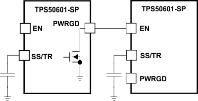
Figure 23 shows the method implementing ratiometric sequencing by connecting the SS/TR pins of two devices together. The regulator outputs ramp up and reach regulation at the same time. When calculating the slow-start time, the pullup current source must be doubled in Equation 7.
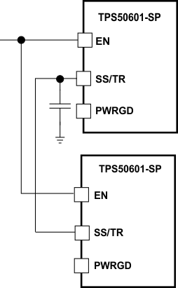 Figure 23. Ratiometric Start-Up Sequence
Ratiometric and simultaneous power-supply sequencing can be implemented by connecting the resistor network of R1 and R2 (shown in Figure 24) to the output of the power supply that needs to be tracked or another voltage reference source. Using Equation 9 and Equation 10, the tracking resistors can be calculated to initiate the Vout2 slightly before, after, or at the same time as Vout1. Equation 11 is the voltage difference between Vout1 and Vout2.
To design a ratiometric start-up in which the Vout2 voltage is slightly greater than the Vout1 voltage when Vout2 reaches regulation, use a negative number in Equation 9 and Equation 10 for ΔV. Equation 11 results in a positive number for applications where the Vout2 is slightly lower than Vout1 when Vout2 regulation is achieved.
The ΔV variable is 0 V for simultaneous sequencing. To minimize the effect of the inherent SS/TR to VSENSE offset (Vssoffset, 29 mV) in the slow-start circuit and the offset created by the pullup current source (Iss, 2 μA) and tracking resistors, the Vssoffset and Iss are included as variables in the equations.
To ensure proper operation of the device, the calculated R1 value from Equation 9 must be greater than the value calculated in Equation 12.


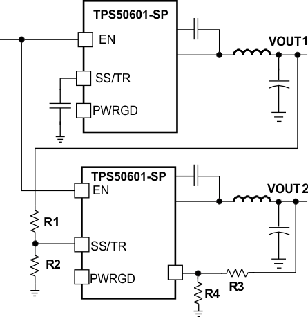 Figure 24. Ratiometric and Simultaneous Start-Up Sequence
8.3.16 Output Overvoltage Protection (OVP)
The device incorporates an output OVP circuit to minimize output voltage overshoot. For example, when the power supply output is overloaded, the error amplifier compares the actual output voltage to the internal reference voltage. If the VSENSE pin voltage is lower than the internal reference voltage for a considerable time, the output of the error amplifier demands maximum output current. After the condition is removed, the regulator output rises and the error amplifier output transitions to the steady-state voltage. In some applications with small output capacitance, the power supply output voltage can respond faster than the error amplifier. This leads to the possibility of an output overshoot. The OVP feature minimizes the overshoot by comparing the VSENSE pin voltage to the OVP threshold. If the VSENSE pin voltage is greater than the OVP threshold, the high-side MOSFET is turned off, preventing current from flowing to the output and minimizing output overshoot. When the VSENSE voltage drops lower than the OVP threshold, the high-side MOSFET is allowed to turn on at the next clock cycle.
8.3.17 Overcurrent Protection
The device is protected from overcurrent conditions by cycle-by-cycle current limiting on both the high-side and low-side MOSFET.
8.3.17.1 High-Side MOSFET Overcurrent Protection
The device implements current mode control which uses the COMP pin voltage to control the turn off of the high-side MOSFET and the turn on of the low-side MOSFET on a cycle-by-cycle basis. Each cycle the switch current and the current reference generated by the COMP pin voltage are compared, when the peak switch current intersects the current reference, the high-side switch is turned off.
8.3.17.2 Low-Side MOSFET Overcurrent Protection
While the low-side MOSFET is turned on its conduction current is monitored by the internal circuitry. During normal operation the low-side MOSFET sources current to the load. At the end of every clock cycle, the low-side MOSFET sourcing current is compared to the internally set low-side sourcing current limit. If the low-side sourcing current is exceeded, the high-side MOSFET is not turned on and the low-side MOSFET stays on for the next cycle. The high-side MOSFET is turned on again when the low-side current is below the low-side sourcing current limit at the start of a cycle.
The low-side MOSFET may also sink current from the load. If the low-side sinking current limit is exceeded, the low-side MOSFET is turned off immediately for the rest of that clock cycle. In this scenario, both MOSFETs are off until the start of the next cycle.
When the low-side MOSFET turns off, the switch node increases and forward biases the high-side MOSFET parallel diode (the high-side MOSFET is still off at this stage).
8.3.18 TPS50601-SP Thermal Shutdown
The internal thermal shutdown circuitry forces the device to stop switching if the junction temperature exceeds 175°C typically. The device reinitiates the power-up sequence when the junction temperature drops below 165°C typically.
8.3.19 Turn-On Behavior
Minimum on-time specification determines the maximum operating frequency of the design. As the unit starts up and goes through its soft-start process, the required duty-cycle is less than the minimum controllable on-time. This can cause the converter to skip pulses. Thus, instantaneous output pulses can be higher or lower than the desired voltage. This behavior is only evident when operating at high frequency with high bandwidth. When the minimum on-pulse is greater than the minimum controllable on-time, the turn-on behavior is normal. When operating at low frequencies (100 kHz or less), the turn-on behavior does not exhibit any ringing at initial startup.
8.3.20 Small Signal Model for Loop Response
Figure 25 shows an equivalent model for the device control loop, which can be modeled in a circuit simulation program to check frequency response and transient responses. The error amplifier is a transconductance amplifier with a gm of 1300 μA/V. The error amplifier can be modeled using an ideal voltage-controlled current source. The resistor, Roea (30 MΩ), and capacitor, Coea (20.7 pF), model the open-loop gain and frequency response of the error amplifier. The 1-mV ac voltage source between the nodes a and b effectively breaks the control loop for the frequency response measurements. Plotting a/c and c/b show the small signal responses of the power stage and frequency compensation respectively. Plotting a/b shows the small signal response of the overall loop. The dynamic loop response can be checked by replacing the RL with a current source with the appropriate load-step amplitude and step rate in a time domain analysis.
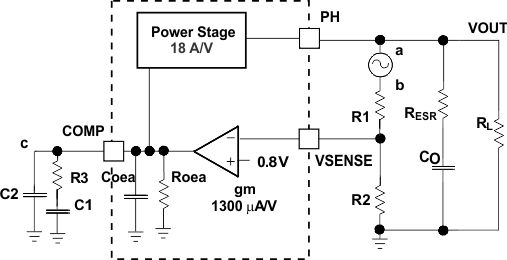 Figure 25. Small Signal Model For Loop Response
8.3.21 Simple Small Signal Model for Peak Current Mode Control
Figure 26 is a simple small signal model that can be used to understand how to design the frequency compensation. The device power stage can be approximated to a voltage-controlled current source (duty cycle modulator) supplying current to the output capacitor and load resistor. Equation 13 shows the control to output transfer function, which consists of a dc gain, one dominant pole, and one ESR zero. The quotient of the change in switch current and the change in COMP pin voltage (node c in Figure 25) is the power stage transconductance (gmps), which is 18 A/V for the device. The dc gain of the power stage is the product of gmps and the load resistance (RL) as shown in Equation 14 with resistive loads. As the load current increases, the dc gain decreases. This variation with load may seem problematic at first glance, but fortunately, the dominant pole moves with load current (see Equation 15). The combined effect is highlighted by the dashed line in Figure 27. As the load current decreases, the gain increases and the pole frequency lowers, keeping the 0-dB crossover frequency the same for the varying load conditions, which makes it easier to design the frequency compensation.
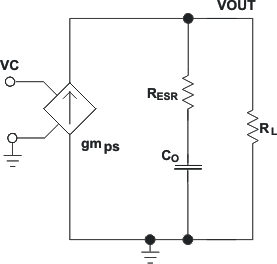 Figure 26. Simplified Small Signal Model for Peak Current Mode Control
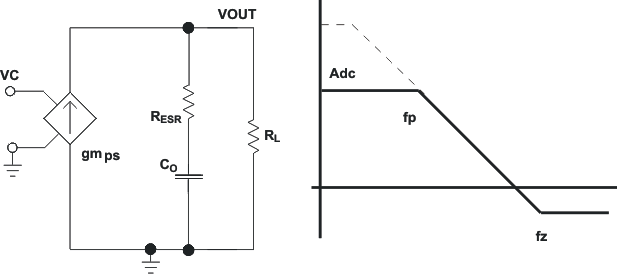 Figure 27. Simplified Frequency Response for Peak Current Mode Control
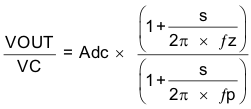


where
- gmea is the GM amplifier gain (1300 μA/V).
- gmps is the power stage gain (18 A/V).
- RL is the load resistance.
- CO is the output capacitance.
- RESR is the equivalent series resistance of the output capacitor.
8.3.22 Small Signal Model for Frequency Compensation
The device uses a transconductance amplifier for the error amplifier and readily supports two of the commonly used frequency compensation circuits shown in Figure 28. In Type 2A, one additional high-frequency pole is added to attenuate high-frequency noise.
The following design guidelines are provided for advanced users who prefer to compensate using the general method. The step-by-step design procedure described in Detailed Design Procedure may also be used.
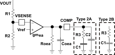 Figure 28. Types of Frequency Compensation
The general design guidelines for device loop compensation are as follows:
- Determine the crossover frequency ƒc. A good starting point is one-tenth of the switching frequency, ƒSW.
- R3 can be determined by:
- gmea is the GM amplifier gain ( 1300 μA/V).
- gmps is the power stage gain (18 A/V).
- Vref is the reference voltage (0.795 V)
- Place a compensation zero at the dominant pole
 .
.
C1 can be determined by - C2 is optional. It can be used to cancel the zero from the equivalent series resistance (ESR) of the output capacitor Co.

where


NOTE
For PSpice models and WEBENCH design tool, see the Tools & Software tab.
- PSpice average model (stability – bode plot)
- PSpice transient model (switching waveforms)
- WEBENCH design tool www.ti.com/product/TPS50601-SP/toolssoftware
8.4 Device Functional Modes
8.4.1 Fixed-Frequency PWM Control
The device uses fixed frequency, peak current mode control. The output voltage is compared through external resistors on the VSENSE pin to an internal voltage reference by an error amplifier which drives the COMP pin. An internal oscillator initiates the turn on of the high-side power switch. The error amplifier output is converted into a current reference which compares to the high-side power switch current. When the power switch current reaches the current reference generated by the COMP voltage level, the high-side power switch is turned off and the low-side power switch is turned on.
8.4.2 Continuous Current Mode (CCM) Operation
As a synchronous buck converter, the device normally works in CCM under all load conditions.