SLVS832D November 2008 – July 2014 TPS22941 , TPS22942 , TPS22943 , TPS22944 , TPS22945
PRODUCTION DATA.
- 1 Features
- 2 Applications
- 3 Description
- 4 Revision History
- 5 Device Comparison Table
- 6 Pin Configuration and Functions
- 7 Specifications
- 8 Detailed Description
- 9 Application and Implementation
- 10Power Supply Recommendations
- 11Layout
- 12Device and Documentation Support
- 13Mechanical, Packaging, and Orderable Information
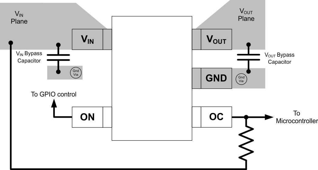
11 Layout
11.1 Layout Guidelines
- For best performance, all traces should be as short as possible.
- To be most effective, the input and output capacitors should be placed close to the device to minimize the effects that parasitic trace inductances may have on normal and short-circuit operation.
- The VIN terminal should be bypassed to grond with low ESR ceramic bypass capacitors. The typical recommended bypass capacitance is 1-µF ceramic with X5R or X7R dielectric. This capacitor should be placed as close to the device terminals as possible.
- The VOUT terminal should be bypassed to grond with low ESR ceramic bypass capacitors. The typical recommended bypass capacitance is one-tenth of the VIN bypass capacitor of X5R or X7R dielectric. This capacitor should be placed as close to the device terminals as possible.
- Using wide traces for VIN, VOUT, and GND will help minimize parasitic electrical effects along with minimizing the case to ambient thermal impedance.
11.2 Layout Example
11.3 Thermal Considerations
The maximum junction temperature will be internally limited by the thermal shutdown (TSD). To calculate the maximum allowable dissipation, PD(MAX) for a given ambient temperature, use Equation 5.
Equation 5. 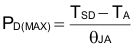
where
- PD(MAX) = maximum allowable power dissipation
- TSD = thermal shutdown threshold (140 °C typical)
- TA = ambient temperature of the device
- θJA = junction to air thermal impedance. See the section. This parameter is highly dependent upon board layout.