ZHCSEF8 December 2015 TPIC2010
PRODUCTION DATA.
- 1 特性
- 2 应用
- 3 说明
- 4 修订历史记录
- 5 说明(续)
- 6 Pin Configuration and Functions
-
7 Specifications
- 7.1 Absolute Maximum Ratings
- 7.2 ESD Ratings
- 7.3 Recommended Operating Conditions
- 7.4 Thermal Information
- 7.5 Electrical Characteristics - Serial Port Voltage Levels
- 7.6 Electrical Characteristics - Common Part
- 7.7 Electrical Characteristics - Charge Pump
- 7.8 Electrical Characteristics - V1pXV DC-DC Converter
- 7.9 Electrical Characteristics - 3.3-V DC-DC Converter
- 7.10 Electrical Characteristics - Spindle Motor Driver Part
- 7.11 Electrical Characteristics - Sled Motor Driver Part
- 7.12 Electrical Characteristics - Focus/Tilt/Tracking/Driver Part
- 7.13 Electrical Characteristics - Load Driver Part
- 7.14 Electrical Characteristics - Stepping Motor Driver Part
- 7.15 Electrical Characteristics - Current Switch Part
- 7.16 Electrical Characteristics - LED Switch Part
- 7.17 Electrical Characteristics - Thermometer Part
- 7.18 Electrical Characteristics - Actuator Protection
- 7.19 Serial Port I/F Write Timing Requirements
- 7.20 Serial Port I/F Read Timing Requirements
- 7.21 Typical Characteristics
-
8 Detailed Description
- 8.1 Overview
- 8.2 Functional Block Diagram
- 8.3 Feature Description
- 8.4 Device Functional Modes
- 8.5 Programming
- 8.6
Register Maps
- 8.6.1 Register State Transition
- 8.6.2 DAC Register (12-Bit Write Only)
- 8.6.3 Control Register (8-Bit Read/Write)
- 8.6.4
Detailed Description of Register
- 8.6.4.1 REG01 12-Bit DAC for Tilt
- 8.6.4.2 REG02 12-Bit DAC for Focus
- 8.6.4.3 REG03 12-Bit DAC for Tracking
- 8.6.4.4 REG04 12-Bit DAC for Sled1
- 8.6.4.5 REG05 12-Bit DAC for Sled2
- 8.6.4.6 REG06 12-Bit DAC for Stepping1
- 8.6.4.7 REG07 12-Bit DAC for Stepping2
- 8.6.4.8 REG08 12-Bit DAC for Spindle
- 8.6.4.9 REG09 12-Bit DAC for Load
- 8.6.4.10 REG63 8-Bit Control Register for SpinAdj
- 8.6.4.11 REG6C 8-Bit Control Register for EDetCfg
- 8.6.4.12 REG6D 8-Bit Control Register for DCCfg
- 8.6.4.13 REG6E 8-Bit Control Register for UtilCfg
- 8.6.4.14 REG6F 8-Bit Control Register for MonitorSet
- 8.6.4.15 REG70 8bit Control Register for DriverEna
- 8.6.4.16 REG71 8-Bit Control Register for FuncEna
- 8.6.4.17 REG72 8-Bit Control Register for ACTCfg
- 8.6.4.18 REG73 8-Bit Control Register for Parm0
- 8.6.4.19 REG74 8-Bit Control Register for SIFCfg
- 8.6.4.20 REG76 8-Bit Control Register for WriteEna
- 8.6.4.21 REG77 8-Bit Control Register for ClrReg
- 8.6.4.22 REG78 8-Bit Control Register for ActTemp
- 8.6.4.23 REG79 8-Bit Control Register for UVLOMon
- 8.6.4.24 REG7A 8-Bit Control Register for ThPMon
- 8.6.4.25 REG7B 8-Bit Control Register for OCPMon
- 8.6.4.26 REG7C 8-Bit Control Register for TempMon
- 8.6.4.27 REG7E 8-Bit Control Register for Version (REG7E)
- 8.6.4.28 REG7F 8-Bit Control Register for Status (REG7F)
-
9 Application and Implementation
- 9.1
Application Information
- 9.1.1 DAC Type
- 9.1.2 Example Sampling Rate of 12-Bit DAC for FCS/TRK/TLT
- 9.1.3 Digital Input Coding
- 9.1.4 Example Timing of Target Control System
- 9.1.5 Spindle Motor Driver Part
- 9.1.6 Sled Driver Part
- 9.1.7 Load Driver Part
- 9.1.8 Focus/Track/Tilt Driver Part
- 9.1.9 2-Channel Synchronous DC-DC Converter
- 9.1.10 Monitor Signal on GPOUT
- 9.2 Typical Application
- 9.1
Application Information
- 10Power Supply Recommendations
- 11Layout
- 12器件和文档支持
- 13机械、封装和可订购信息
7 Specifications
7.1 Absolute Maximum Ratings
see (1)(3)| MIN | MAX | UNIT | ||
|---|---|---|---|---|
| 5-V supply voltage A5V, P5V | 6 | V | ||
| Spindle output peak voltage(4) | 7 | V | ||
| Input/output voltage | –0.3 | VCC + 0.3 V | V | |
| Spindle output current | 1.0 | A | ||
| Spindle output peak current (PW ≦ 2 ms, Duty ≦ 30%) | 2.5 | A | ||
| Sled output peak current | 0.8 | A | ||
| Focus/tilt/tracking driver output peak current | 1.5 | A | ||
| Load driver output peak current | 0.8 | A | ||
| Power dissipation(2) | 1344 | mW | ||
| Operating temperature | –20 | 75 | °C | |
| Tstg | Storage temperature | –50 | 150 | °C |
(1) Stresses beyond those listed under Absolute Maximum Ratings may cause permanent damage to the device. These are stress ratings only, which do not imply functional operation of the device at these or any other conditions beyond those indicated under Recommended Operating Conditions. Exposure to absolute-maximum-rated conditions for extended periods may affect device reliability.
(2) A lower RθJC is attainable if the exposed pad is connected to a large copper ground plane. RθJC and RθJA are values for 56-pin TSSOP without a exposed heat slug (HSL) on bottom. Actual thermal resistance would be better than the above values.
(3) All voltage values are with respect to the GND.
(4) The output voltage generated with regeneration current at the time of output is off states.
7.2 ESD Ratings
| VALUE | UNIT | |||
|---|---|---|---|---|
| V(ESD) | Electrostatic discharge | Human-body model (HBM), per ANSI/ESDA/JEDEC JS-001(1) | ±2000 | V |
| Charged-device model (CDM), per JEDEC specification JESD22-C101(2) | ±500 | |||
(1) JEDEC document JEP155 states that 500-V HBM allows safe manufacturing with a standard ESD control process.
(2) JEDEC document JEP157 states that 250-V CDM allows safe manufacturing with a standard ESD control process.
7.3 Recommended Operating Conditions
| MIN | NOM | MAX | UNIT | ||
|---|---|---|---|---|---|
| A5V | Operating supply voltage (apply for A5V) | 4.5 | 5.0 | 5.5 | V |
| P5V | Driver 5V supply voltage (apply for P5V) | A5V – 0.2 | A5V | A5V + 0.2 | V |
| CSWIV | CSWI input voltage (apply for P5V) | A5V – 0.2 | A5V | A5V + 0.2 | V |
| VSIOV | SIOV voltage | 3.0 | 3.3 | 3.6 | V |
| VSIFH | SIMO, SSZ, SCLK pin “H” level input voltage range | 2.2 | SIOV + 0.2 | V | |
| VSIFL | SIMO, SSZ, SCLK pin “L” level input voltage range | –0.2 | 0.8 | V | |
| VIHB | XMUTE, SWR_SEQ1, SWR_SEQ2, V1pXSEL pin “H” level input voltage |
2.2 | A5V + 0.1 | V | |
| VILB | XMUTE, SWR_SEQ1, SWR_SEQ2, V1pXSEL pin “L” level input voltage range |
–0.1 | 0.8 | V | |
| ISPMOA | Spindle output average current (U, V, W total) | 700 | mA | ||
| ISPMO | Spindle output current | 700 | mA | ||
| ISLDOA | Sled output average current | 400 | mA | ||
| ILd1Px | 1pXV switching regulator load current | 900 | mA | ||
| ILd3P3 | 3p3V switching regulator load current | 500 | mA | ||
| IACTOA | Focus / tracking / tilt / loading output average current | 400 | mA | ||
| ICSWOA | CSWO output average current | 200 | mA | ||
| ISTPOA | STP output average current | 200 | mA | ||
| Fck | SCLK frequency | 30 | 33.8688 | 35 | MHz |
| TO | Operating temperature range | –20 | 25 | 75 | °C |
7.4 Thermal Information
| THERMAL METRIC(1) | TPIC2010 | UNIT | |
|---|---|---|---|
| DFD (HTSSOP) | |||
| 56 PINS | |||
| RθJA | Junction-to-ambient thermal resistance | 16.9 | °C/W |
| RθJC(top) | Junction-to-case (top) thermal resistance | 0.8 | °C/W |
| RθJB | Junction-to-board thermal resistance | 5.2 | °C/W |
| ψJT | Junction-to-top characterization parameter | 1.0 | °C/W |
| ψJB | Junction-to-board characterization parameter | 5.2 | °C/W |
| RθJC(bot) | Junction-to-case (bottom) thermal resistance | 0.9 | °C/W |
(1) For more information about traditional and new thermal metrics, see the Semiconductor and IC Package Thermal Metrics application report, SPRA953.
7.5 Electrical Characteristics – Serial Port Voltage Levels
over recommended operating free-air temperature range (A5V ≈ 4.5 to 5.5 V, P5V_1, P5V_2, P5V_STP, P5V_SPM1, P5V_SPM2 = A5V, VREF = 1.65 V, TA ≈ –20°C to 75°C; unless otherwise noted)| PARAMETER | TEST CONDITIONS | MIN | TYP | MAX | UNIT | |
|---|---|---|---|---|---|---|
| SOMI | High-level output voltage, VOH | IOH = 1 mA | 80% SPIOV |
V | ||
| SOMI | Low-level output voltage, VOL | IOL = 1 mA | 20% SPIOV |
V | ||
| SIMO | High-level input voltage, VIH | 70% SPIOV |
V | |||
| SIMO | Low level input voltage, VIL | 20% SPIOV |
V | |||
| SIMO | Input rise/fall time | 10% → 90% PIOV | 3.5 | ns | ||
| SIMO | Output rise/fall time(1) | Cload = 30 pF,10% → 90% SPIOV | 10 | ns | ||
| SCLK | Internal pulldown resistance | 200 | kΩ | |||
| SSZ | Internal pullup resistance | 200 | kΩ | |||
(1) Specified by design
7.6 Electrical Characteristics – Common Part
over recommended operating free-air temperature range (A5V ≈ 4.5 to 5.5 V, P5V_1, P5V_2, P5V_STP, P5V_SPM1, P5V_SPM2 = A5V, VREF = 1.65 V, TA ≈ –20°C to 75°C; unless otherwise noted)| PARAMETER | TEST CONDITIONS | MIN | TYP | MAX | UNIT | |
|---|---|---|---|---|---|---|
| ISTBY | Stand by Supply current | SWR_SEQ1 = SWR_SEQ2 = V1PxSEL = A5V | 1 | mA | ||
| VCV3 | CV3P3 Output voltage | Iload = 25 mA | 3.135 | 3.3 | 3.465 | V |
| RXM | XMUTE pulldown resistor | 100 | 200 | 300 | kΩ | |
| RSW1 | SWR_SEQ1 pulldown resistor | 100 | 200 | 300 | kΩ | |
| RSW2 | SWR_SEQ2 pulldown resistor | 100 | 200 | 300 | kΩ | |
| RSELS1 | V1PxSEL pulldown resistor | 100 | 200 | 300 | kΩ | |
| RXRST | XRESET pullup resistor | 16.5 | 33 | 49.5 | kΩ | |
| VXRST | XRESET low level output voltage | SIOV = 3.3 V, IOL = –100 µA | 0.3 | V | ||
| TPOR | Power-On Reset delay | 15 | 20 | 25 | ms | |
| RXFG | XFG output resistor | 100 | 200 | 300 | Ω | |
| VXFGH | XFG high level output voltage | SIOV = 3.3 V, XSLEEP = 1, IOH = 100 µA |
2.7 | V | ||
| VXFGL | XFG low level output voltage | SIOV = 3.3 V, XSLEEP = 1, IOL = –100 µA |
0.3 | V | ||
| RGPO | GPOUT output resistor | 100 | 200 | 300 | Ω | |
| VGPOH | GPOUT high level output voltage | SIOV = 3.3 V, XSLEEP = 1, GPOUT_ENA = 1, GPOUT_HL = 1, IOH = 100 µA |
2.7 | V | ||
| VGPOL | GPOUT low level output voltage | SIOV = 3.3 V, XSLEEP = 1, GPOUT_ENA = 1,GPOUT_HL = 0, IOH = 100 µA |
0.3 | V | ||
| tTSD | Thermal protect on temperature | Design ensured value | 130 | 145 | 165 | ºC |
| hytTSD | Thermal protect hys temperature | 5 | 15 | 25 | ºC | |
| Vonvcc | A5V Reset on voltage | 3.6 | 3.7 | 3.8 | V | |
| Voffvcc | A5V Reset off voltage | 3.8 | 3.9 | 4 | V | |
| VonCV3 | CV3P3 reset on voltage | 2.6 | 2.7 | 2.8 | V | |
| VoffCV3 | CV3P3 reset off voltage | 2.68 | 2.8 | 2.88 | V | |
| HysCV3 | CV3P3 reset voltage Hys | 35 | 85 | 135 | mV | |
| VovpspmOn | OVP detection voltage (Spindle)(1) | 6 | 6.2 | 6.4 | V | |
| VovpspmOff | OVP release voltage (Spindle)(1) | 5.8 | 6 | 6.2 | V | |
| VovpSpmHys | OVP voltage Hys (Spindle)(1) | 140 | 240 | 340 | mV | |
| VovpOn | OVP detection voltage (except Spindle)(1) |
6.3 | 6.5 | 6.7 | V | |
| VovpOff | OVP release voltage (except Spindle)(1) |
6.1 | 6.3 | 6.5 | V | |
| VovpHys | OVP voltage Hys (except Spindle)(1) |
140 | 240 | 340 | mV | |
(1) Those are value as protection functions only, and stress beyond those listed under Recommended Operating Conditions may cause permanent damage to the device.
7.7 Electrical Characteristics – Charge Pump
over recommended operating free-air temperature range (A5V ≈ 4.5 to 5.5 V, P5V_1, P5V_2, P5V_STP, P5V_SPM1, P5V_SPM2 = A5V, VREF = 1.65 V, TA ≈ –20°C to 75°C; unless otherwise noted)| PARAMETER | TEST CONDITIONS | MIN | TYP | MAX | UNIT | |
|---|---|---|---|---|---|---|
| FCHGP | Frequency | XSLEEP=1 | 132.6 | 156 | 179.4 | kHz |
| VCHGP | Output Voltage | Ccp1 = Ccp3 = 0.1 µF Io = –1 mA |
7.76 | 9.7 | 11.64 | V |
7.8 Electrical Characteristics – V1pXV DC-DC Converter
over recommended operating free-air temperature range (A5V ≈ 4.5 to 5.5 V, P5V_1, P5V_2, P5V_STP, P5V_SPM1, P5V_SPM2 = A5V, VREF = 1.65 V, TA ≈ –20°C to 75°C; unless otherwise noted)| PARAMETER | TEST CONDITIONS | MIN | TYP | MAX | UNIT | |
|---|---|---|---|---|---|---|
| Rds1pxH | High-side FET RDSON | FB1PXV = 0 V REG1PXV + 100 mA, +300 mA | 0.42 | 0.62 | Ω | |
| Rds1pxL | Low-side FET RDSON | FB1PXV = 1.2 V REG1PXV –100 mA , –300 mA | 0.2 | 0.4 | Ω | |
| VO1p0 | Output voltage (1p0V) | [V1PxSEL,SWR_SEQ1,SWR_SEQ2] = 011 | 0.95 | 1 | 1.05 | V |
| VO1p2 | Output voltage (1p2V) | [V1PxSEL,SWR_SEQ1,SWR_SEQ2] = 000 | 1.14 | 1.2 | 1.26 | V |
| VO1p5 | Output voltage (1p5V) | [V1PxSEL,SWR_SEQ1,SWR_SEQ2] = 100 | 1.425 | 1.5 | 1.575 | V |
| Tdly1px | Soft start time | [SWR_SEQ1,SWR_SEQ2] = 00 From A5V reset off to target 90% |
0.656 | 0.82 | 0.984 | ms |
| RdsO1px | Output pulldown transistor Rdson | At Reset On (TSD, A5V_Reset) | 616 | 880 | 1144 | Ω |
| Fsw1px | Switching frequency | 2.125 | 2.5 | 2.875 | MHz | |
| Vrston1px | Reset on voltage threshold level | 75% | 80% | 85% | ||
| Vrstoff1px | Reset off voltage threshold level | 85% | 90% | 95% | ||
| VrstHys | Reset off voltage threshold Hys | 5% | 10% | 15% | ||
| PSRR1px | PSRR ratio | P5V_SW = 5 V + 200 mVpp, Io = 200 mA, F ≈ 100 kHz |
26 | dB | ||
| Iovc1px | Overcurrent protective level(1) | 1.3 | 1.85 | 2.4 | A | |
| TMskovc1px | Mask time of overcurrent protection(1) | 0.72 | 1 | 1.32 | ms | |
(1) Those are value as protection functions only, and stress beyond those listed under Recommended Operating Conditions may cause permanent damage to the device.
7.9 Electrical Characteristics – 3.3-V DC-DC Converter
over recommended operating free-air temperature range (A5V ≈ 4.5 to 5.5 V, P5V_1, P5V_2, P5V_STP, P5V_SPM1, P5V_SPM2 = A5V, VREF = 1.65 V, TA ≈ –20°C to 75°C; unless otherwise noted)| PARAMETER | TEST CONDITIONS | MIN | TYP | MAX | UNIT | |
|---|---|---|---|---|---|---|
| Rds3p3H | High-side FET RDSON | FB3P3V = 0 V REG3P3V + 100 mA + 300 mA | 0.45 | 0.65 | Ω | |
| Rds3p3L | Low-side FET RDSON | FB3P3V = 3.3 V REG3P3V –100 mA – 300 mA | 0.42 | 0.62 | Ω | |
| VO3p3 | Output voltage | 3.2 | 3.3 | 3.4 | V | |
| Tdly3p3 | Soft start time | [SWR_SEQ1,SWR_SEQ2] = 00 From A5V reset off to target 90% |
0.656 | 0.82 | 0.984 | ms |
| Rds3p3 | Output pull down transistor Rdson | At reset on (TSD, A5V_Reset) | 616 | 880 | 1144 | Ω |
| Fsw3p3 | Switching frequency | 2.125 | 2.5 | 2.875 | MHz | |
| Vrston3p3 | Reset on voltage threshold level | 75% | 80% | 85% | ||
| Vrstoff3p3 | Reset off voltage threshold level | 85% | 90% | 95% | ||
| Vrst3p3Hys | Reset off voltage threshold Hys | 5% | 10% | 15% | ||
| PSRR3p3 | PSRR ratio | P5V_SW = 5 V + 200 mVpp, Io = 200 mA, F ≈ 100 kHz |
26 | dB | ||
| Iovc3p3 | Overcurrent protective level(1) | 0.65 | 1.15 | 1.65 | A | |
| Tmskovc3p3 | Mask time of overcurrent protection(1) | 0.72 | 1 | 1.32 | ms | |
(1) Data are value as protection functions only, and stress beyond those listed under “Recommended Operating Condition” may cause permanent damage to the device.
7.10 Electrical Characteristics – Spindle Motor Driver Part
over recommended operating free-air temperature range (A5V ≈ 4.5 to 5.5 V, P5V_1, P5V_2, P5V_STP, P5V_SPM1, P5V_SPM2 = A5V, VREF = 1.65 V, TA ≈ –20°C to 75°C; unless otherwise noted)| PARAMETER | TEST CONDITIONS | MIN | TYP | MAX | UNIT | |
|---|---|---|---|---|---|---|
| RttlSPM | Total output resistance High side + low side |
IOUT = 0.1 A | 0.25 | 0.5 | Ω | |
| VIsns | ISENSE detected voltage | ISENSE voltage | 181 | 196 | 211 | mV |
| ResSPM | Resolution | 12 | bit | |||
| VoutSPM | Spindle voltage | VSPM(REG8h) = 400h | 2.6 | 3 | 3.4 | V |
| VSPM(REG8h) = C00h | –1.55 | –1.25 | –0.95 | V | ||
| WidDZSPM | Spindle dead band | Forward | +12h | +52h | +92h | |
| Reverse | –92h | –52h | –12h | |||
| WidDZSPMLS | Spindle dead band (LS mode) | –40h | 0h | 40h | ||
7.11 Electrical Characteristics – Sled Motor Driver Part
over recommended operating free-air temperature range (A5V ≈ 4.5 to 5.5 V, P5V_1, P5V_2, P5V_STP, P5V_SPM1, P5V_SPM2 = A5V, VREF = 1.65 V, TA ≈ –20°C to 75°C; unless otherwise noted)| PARAMETER | TEST CONDITIONS | MIN | TYP | MAX | UNIT | |
|---|---|---|---|---|---|---|
| RttlSLD | Total output resistance High side + low side |
IO = 0.1 A | 0.7 | 1.1 | Ω | |
| ResSLD | Resolution | 10 | bit | |||
| WidDZSLD | Input dead band | Forward | +4h | +51h | +90h | |
| Reverse | –90h | –51h | –4h | |||
| GnSLD | Sled current gain | A5V = 5 V, 5 V = 5 V RL = 10 Ω, 2.2 mH VSLED = 7FFh |
380 | 440 | 500 | mA |
| VthEdetSLD | END_DET BEMF threshold voltage | ENDDET_SLCT = 0, SLEDENDTH<1:0> = 00, SLED Enable | 26 | 46 | 66 | mV |
7.12 Electrical Characteristics – Focus/Tilt/Tracking/Driver Part
over recommended operating free-air temperature range (A5V ≈ 4.5 to 5.5 V, P5V_1, P5V_2, P5V_STP, P5V_SPM1, P5V_SPM2 = A5V, VREF = 1.65 V, TA ≈ –20°C to 75°C; unless otherwise noted)| PARAMETER | TEST CONDITIONS | MIN | TYP | MAX | UNIT | |
|---|---|---|---|---|---|---|
| RttlAct | Total output resistance High side + low side |
IO = 0.1 A | 0.7 | 1.1 | Ω | |
| ResACT | Resolution | 12 | bit | |||
| VOfstACT | Each channel output offset voltage | DAC_code = 000h | –30 | 0 | 30 | mV |
| VOfstDACT | Output offset voltage Focus and Tilt | DIFF_TLT = 1 | –50 | 0 | 50 | mV |
| GnDAct | Difference gain Focus and Tilt | DIFF_TLT = 1 | –1 | 0 | 1 | db |
| GnAct | Voltage gain | DAC_code = 400h | 2.6 | 3 | 3.4 | V |
| DAC_code = C00h | –3.4 | –3 | –2.6 | |||
7.13 Electrical Characteristics – Load Driver Part
over recommended operating free-air temperature range (A5V ≈ 4.5 to 5.5 V, P5V_1, P5V_2, P5V_STP, P5V_SPM1, P5V_SPM2 = A5V, VREF = 1.65 V, TA ≈ –20°C to 75°C; unless otherwise noted)| PARAMETER | TEST CONDITIONS | MIN | TYP | MAX | UNIT | |
|---|---|---|---|---|---|---|
| RttlLOD | Total output resistance High side + low side |
IO = 0.1 A | 0.7 | 1.1 | Ω | |
| ResLOD | Resolution | 12 | bit | |||
| GnLOD | Voltage gain | VLOAD = 400h | 2.6 | 3 | 3.4 | V |
| VLOAD = C00h | –3.4 | –3 | –2.6 | |||
| WidDZLOD | Dead band | Forward | 2h | 20h | 40h | |
| Reverse | –41h | –21h | –3h | |||
| TocpLOD | Output 100% limit time | LOAD_05CH = 0 | 0.64 | 0.8 | 0.96 | s |
| IocpLOD | Overcurrent protective level | LOAD_05CH = 1 | 125 | 250 | 375 | mA |
| DlyocpLOD | Overcurrent protection delay time | LOAD_05CH = 1 | 0.64 | 0.8 | 0.96 | s |
7.14 Electrical Characteristics – Stepping Motor Driver Part
over recommended operating free-air temperature range (A5V ≈ 4.5 to 5.5 V, P5V_1, P5V_2, P5V_STP, P5V_SPM1, P5V_SPM2 = A5V, VREF = 1.65 V, TA ≈ –20°C to 75°C; unless otherwise noted)| PARAMETER | TEST CONDITIONS | MIN | TYP | MAX | UNIT | |
|---|---|---|---|---|---|---|
| RttlSTP | Total output resistance High Side + Low Side |
IO = 0.1 A | 1.0 | 1.5 | Ω | |
| ResSTP | Resolution | 8 | bit | |||
| IocpSTP | Overcurrent protection level(1) | 595 | 850 | 1105 | mA | |
| DlyocpSTP | OCP Monitor delay time(1) | 0.7 | 1 | 1.3 | us | |
| ThlocpSTP | OCP hold time(1) | 18.2 | 26 | 33.8 | ms | |
| VthEdetSTP | END_DET threshold level | ENDDET_SLCT = 1, STPDENDTH<1:0> = 00, STP Enable | 19 | 39 | 59 | mV |
(1) The data are value as protection functions only, and stress beyond those listed under Recommended Operating Conditions may cause permanent damage to the device.
7.15 Electrical Characteristics – Current Switch Part
over recommended operating free-air temperature range (A5V ≈ 4.5 to 5.5 V, P5V_1, P5V_2, P5V_STP, P5V_SPM1, P5V_SPM2 = A5V, VREF = 1.65 V, TA ≈ –20°C to 75°C; unless otherwise noted)| PARAMETER | TEST CONDITIONS | MIN | TYP | MAX | UNIT | |
|---|---|---|---|---|---|---|
| RdsCSW | Rds(on) | IO = 0.1 A | 200 | 500 | mΩ | |
| IlmtCSW | Current limit threshold level | 0.77 | 1.1 | 1.43 | A | |
| ThlCSW | Protection hold time | 1.47 | 1.6 | 2.0 | ms | |
7.16 Electrical Characteristics – LED Switch Part
over recommended operating free-air temperature range (A5V ≈ 4.5 to 5.5 V, P5V_1, P5V_2, P5V_STP, P5V_SPM1, P5V_SPM2 = A5V, VREF = 1.65 V, TA ≈ –20°C to 75°C; unless otherwise noted)| PARAMETER | TEST CONDITIONS | MIN | TYP | MAX | UNIT | |
|---|---|---|---|---|---|---|
| RdsLED | Rds(on) | IO = 10 mA | 4.4 | 10 | Ω | |
| IlmtLED | Current limit threshold level | 0.07 | 0.1 | 0.13 | A | |
| ThlLED | Protection hold time | 0.37 | 0.4 | 0.66 | ms | |
7.17 Electrical Characteristics – Thermometer Part
over recommended operating free-air temperature range (A5V ≈ 4.5 to 5.5 V, P5V_1, P5V_2, P5V_STP, P5V_SPM1, P5V_SPM2 = A5V, VREF = 1.65 V, TA ≈ –20°C to 75°C; unless otherwise noted)| PARAMETER | TEST CONDITIONS | MIN | TYP | MAX | UNIT | |
|---|---|---|---|---|---|---|
| ResTEMP | Resolution | 6 | bit | |||
| TEMPrng | Temperature range | CHIPTEMP[5:0] = 00 | 8 | 15 | 22 | °C |
| CHIPTEMP[5:0] = 3Fh | 155 | 165 | 175 | |||
| FTEMP | Update cycle | 8 | 10 | 12 | kHz | |
7.18 Electrical Characteristics – Actuator Protection
over recommended operating free-air temperature range (A5V ≈ 4.5 to 5.5 V, P5V_1, P5V_2, P5V_STP, P5V_SPM1, P5V_SPM2 = A5V, VREF = 1.65 V, TA ≈ –20°C to 75°C; unless otherwise noted)| PARAMETER | TEST CONDITIONS | MIN | TYP | MAX | UNIT | |
|---|---|---|---|---|---|---|
| TintACTTEMP | Update cycle | 21 | 26 | 31 | ms | |
7.19 Serial Port I/F Write Timing Requirements
| MIN | NOM | MAX | UNIT | |||
|---|---|---|---|---|---|---|
| Fck | SCLK clock frequency | PIOV = 3.3 V | 35 | MHz | ||
| tckl | SCLK low time | 11 | ns | |||
| tckh | SCLK high time | 11 | ns | |||
| tsens | SSZ setup time | 7 | ns | |||
| tsenh | SSZ hold time | 7 | ns | |||
| tsl | SSZ disable high time | 11 | ns | |||
| tds | SIMO setup time (Write) | 7 | ns | |||
| tdh | SIMO hold time (Write) | 7 | ns | |||
7.20 Serial Port I/F Read Timing Requirements
| MIN | NOM | MAX | UNIT | |||
|---|---|---|---|---|---|---|
| Fck | SCLK clock frequency | PIOV = 3.3 V | 35 | MHz | ||
| tckl | SCLK low time | 11 | ns | |||
| tckh | SCLK high time | 11 | ns | |||
| tsens | SSZ setup time | 7 | ns | |||
| tsenh | SSZ hold time | 7 | ns | |||
| tsl | SSZ disable high time | 11 | ns | |||
| tds | SIMO setup time (Write) | 7 | ns | |||
| tdh | SIMO hold time (Write) | 7 | ns | |||
| trdly | SOMI delay time (Read) | CLOAD = 10 pF, PIOV = 3.3 V | 2 | 9 | ns | |
| tsendl | SOMI hold time (Read) | CLOAD = 10 pF, PIOV = 3.3 V | 2 | 9 | ns | |
| trls | SOMI release time (Read) | CLOAD = 10 pF, PIOV = 3.3 V From SSZ rise to SOMI HIZ |
0 | 9 | ns | |
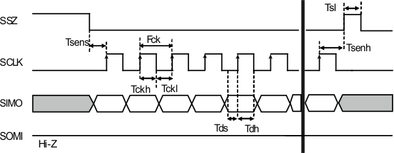 Figure 1. Serial Port Write Timing
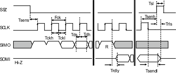 Figure 2. Serial Port Read Timings
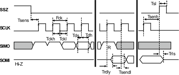 Figure 3. Serial Port Read Timings (ADVANCE_RD Mode)
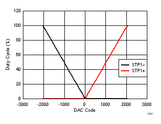
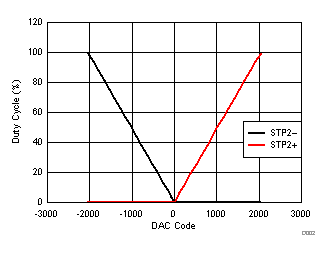
7.21 Typical Characteristics
