ZHCSGS3 April 2017 TPD2S300
PRODUCTION DATA.
- 1 特性
- 2 应用
- 3 说明
- 4 修订历史记录
- 5 Pin Configuration and Functions
- 6 Specifications
-
7 Detailed Description
- 7.1 Overview
- 7.2 Functional Block Diagram
- 7.3
Feature Description
- 7.3.1 2-Channels of Short-to-VBUS Overvoltage Protection (CC1, CC2 Pins): 24-VDC Tolerant
- 7.3.2 2-Channels of IEC61000-4-2 ESD Protection (CC1, CC2 Pins)
- 7.3.3 Low Quiescent Current: 3.23 µA (Typical), VPWR, VM = 3.3 V
- 7.3.4 CC1, CC2 Overvoltage Protection FETs 200 mA Capable for Passing VCONN Power
- 7.3.5 CC Dead Battery Resistors Integrated for Handling Dead Battery Use Case in Mobile Devices
- 7.3.6 1.4-mm × 1.4-mm WCSP Package
- 7.4 Device Functional Modes
- 8 Application and Implementation
- 9 Power Supply Recommendations
- 10Layout
- 11器件和文档支持
- 12机械、封装和可订购信息
5 Pin Configuration and Functions
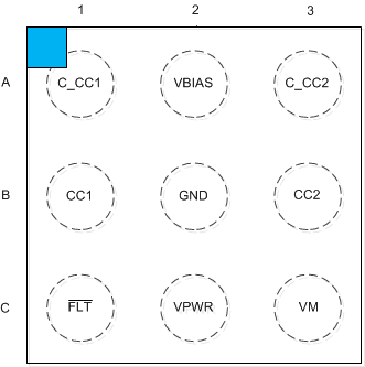
YFF Package
9-Pin WCSP
Top Side Marking View

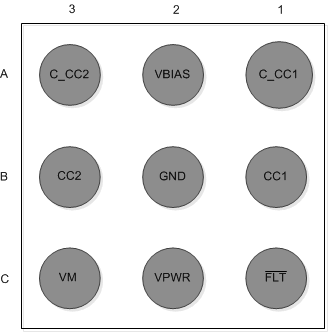
YFF Package
9-Pin WCSP
Bottom, Bump View

Pin Functions
| PIN | TYPE | DESCRIPTION | |
|---|---|---|---|
| NO. | NAME | ||
| A1 | C_CC1 | I/O | Connector side of the CC1 OVP FET. Connect to either CC pin of the USB Type-C connector |
| A2 | VBIAS | Power | Pin for ESD support capacitor. Place a 0.1-µF capacitor on this pin to ground |
| A3 | C_CC2 | I/O | Connector side of the CC2 OVP FET. Connect to either CC pin of the USB Type-C connector |
| B1 | CC1 | I/O | System side of the CC1 OVP FET. Connect to either CC pin of the CC/PD controller |
| B2 | GND | GND | Ground |
| B3 | CC2 | I/O | System side of the CC2 OVP FET. Connect to either CC pin of the CC/PD controller |
| C1 | FLT | O | Open drain for fault reporting |
| C2 | VPWR | Power | 2.7 V–4.5 V power supply |
| C3 | VM | I | Voltage mode pin. Place 2.7 V–4.5 V on pin to operate for CC, PD, and FRS. Place 8.7 V–22 V on pin to operate the device in low resistance mode as well |