SLOS488F November 2006 – March 2015 TPA6130A2
PRODUCTION DATA.
- 1 Features
- 2 Applications
- 3 Description
- 4 Simplified Schematic
- 5 Revision History
- 6 Pin Configuration and Functions
- 7 Specifications
- 8 Detailed Description
- 9 Applications and Implementation
- 10Power Supply Recommendations
- 11Layout
- 12Device and Documentation Support
- 13Mechanical, Packaging, and Orderable Information
封装选项
机械数据 (封装 | 引脚)
散热焊盘机械数据 (封装 | 引脚)
- RTJ|20
订购信息
9 Applications and Implementation
NOTE
Information in the following applications sections is not part of the TI component specification, and TI does not warrant its accuracy or completeness. TI’s customers are responsible for determining suitability of components for their purposes. Customers should validate and test their design implementation to confirm system functionality.
9.1 Application Information
The TPA6130A2 is a stereo DirectPath™ headphone amplifier with I2C digital volume control. The TPA6130A2 has minimal quiescent current consumption, with a typical IDD of 4 mA, making it optimal for portable applications.
9.2 Typical Application
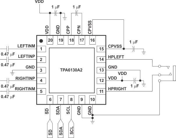
Figure 45 shows a typical application circuit for the TPA6130A2 with a stereo headphone jack and supporting power supply decoupling capacitors.
9.2.1 Design Requirements
For this design example, use the following as the input parameters.
Table 9. Design Parameters
| DESIGN PARAMTER | EXAMPLE VALUE |
|---|---|
| Input voltage | 2.5 V – 5.5 V |
| Minimum current limit | 4 mA |
| Maximum current limit | 6 mA |
9.2.2 Detailed Design Procedure
9.2.2.1 Input-Blocking Capacitors
DC input-blocking capacitors block the dc portion of the audio source, and allow the inputs to properly bias. Maximum performance is achieved when the inputs of the TPA6130A2 are properly biased. Performance issues such as pop are optimized with proper input capacitors.
The dc input-blocking capacitors may be removed provided the inputs are connected differentially and within the input common mode range of the amplifier, the audio signal does not exceed ±3 V, and pop performance is sufficient.
CIN is a theoretical capacitor used for mathematical calculations only. Its value is the series combination of the dc input-blocking capacitors, C(DCINPUT-BLOCKING). Use Equation 1 to determine the value of C(DCINPUT-BLOCKING). For example, if CIN is equal to 0.22 μF, then C(DCINPUT-BLOCKING) is equal to about 0.47 μF.

The two C(DCINPUT-BLOCKING) capacitors form a high-pass filter with the input impedance of the TPA6130A2. Use Equation 1 to calculate CIN, then calculate the cutoff frequency using CIN and the differential input impedance of the TPA6130A2, RIN, using Equation 2. Note that the differential input impedance changes with gain. See Figure 33 for input impedance values. The frequency and/or capacitance can be determined when one of the two values are given.

If a high pass filter with a -3 dB point of no more than 20 Hz is desired over all gain settings, the minimum impedance would be used in the above equation. Figure 33 shows this to be 37 kΩ. The capacitor value by the above equation would be 0.215 μF. However, this is CIN, and the desired value is for C(DCINPUT-BLOCKING). Multiplying CIN by 2 yields 0.43 μF, which is close to the standard capacitor value of 0.47 μF. Place 0.47 μF capacitors at each input terminal of the TPA6130A2 to complete the filter.
9.2.2.2 Charge Pump Flying Capacitor and CPVSS Capacitor
The charge pump flying capacitor serves to transfer charge during the generation of the negative supply voltage. The CPVSS capacitor must be at least equal to the flying capacitor in order to allow maximum charge transfer. Low ESR capacitors are an ideal selection, and a value of 1 µF is typical.
9.2.2.3 Decoupling Capacitors
The TPA6130A2 is a DirectPath™ headphone amplifier that requires adequate power supply decoupling to ensure that the noise and total harmonic distortion (THD) are low. Use good low equivalent-series-resistance (ESR) ceramic capacitors, typically 1.0 µF. Find the smallest package possible, and place as close as possible to the device VDD lead. Placing the decoupling capacitors close to the TPA6130A2 is important for the performance of the amplifier. Use a 10 μF or greater capacitor near the TPA6130A2 to filter lower frequency noise signals. The high PSRR of the TPA6130A2 will make the 10 μF capacitor unnecessary in most applications.
9.2.2.4 I2C Control Interface Details
9.2.2.4.1 Addressing the TPA6130A2
The device operates only as a slave device whose address is 1100000 binary.
9.2.2.5 Headphone Amplifiers
Single-supply headphone amplifiers typically require dc-blocking capacitors. The capacitors are required because most headphone amplifiers have a dc bias on the outputs pin. If the dc bias is not removed, the output signal is severely clipped, and large amounts of dc current rush through the headphones, potentially damaging them. The top drawing in Figure 34 illustrates the conventional headphone amplifier connection to the headphone jack and output signal.
DC blocking capacitors are often large in value. The headphone speakers (typical resistive values of 16 Ω or 32 Ω) combine with the dc blocking capacitors to form a high-pass filter. Equation 3 shows the relationship between the load impedance (RL), the capacitor (CO), and the cutoff frequency (fC).

CO can be determined using Equation 4, where the load impedance and the cutoff frequency are known.

If fc is low, the capacitor must then have a large value because the load resistance is small. Large capacitance values require large package sizes. Large package sizes consume PCB area, stand high above the PCB, increase cost of assembly, and can reduce the fidelity of the audio output signal.
9.2.3 Application Performance Curves
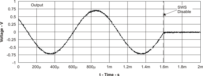
 Figure 46. Shutdown Time
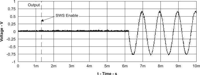
 Figure 47. Startup Time
