ZHCSFK3A February 2016 – October 2016 TPA3255
PRODUCTION DATA.
- 1 特性
- 2 应用
- 3 说明
- 4 修订历史记录
- 5 Device Comparison Table
- 6 Pin Configuration and Functions
-
7 Specifications
- 7.1 Absolute Maximum Ratings
- 7.2 ESD Ratings
- 7.3 Recommended Operating Conditions
- 7.4 Thermal Information
- 7.5 Electrical Characteristics
- 7.6 Audio Characteristics (BTL)
- 7.7 Audio Characteristics (SE)
- 7.8 Audio Characteristics (PBTL)
- 7.9 Typical Characteristics, BTL Configuration
- 7.10 Typical Characteristics, SE Configuration
- 7.11 Typical Characteristics, PBTL Configuration
- 8 Parameter Measurement Information
-
9 Detailed Description
- 9.1 Overview
- 9.2 Functional Block Diagrams
- 9.3 Feature Description
- 9.4
Device Functional Modes
- 9.4.1
Device Protection System
- 9.4.1.1 Overload and Short Circuit Current Protection
- 9.4.1.2 Signal Clipping and Pulse Injector
- 9.4.1.3 DC Speaker Protection
- 9.4.1.4 Pin-to-Pin Short Circuit Protection (PPSC)
- 9.4.1.5 Overtemperature Protection OTW and OTE
- 9.4.1.6 Undervoltage Protection (UVP) and Power-on Reset (POR)
- 9.4.1.7 Fault Handling
- 9.4.1.8 Device Reset
- 9.4.1
Device Protection System
- 10Application and Implementation
- 11Power Supply Recommendations
- 12Layout
- 13器件和文档支持
- 14机械、封装和可订购信息
11 Power Supply Recommendations
11.1 Power Supplies
The TPA3255 device requires two external power supplies for proper operation. A high-voltage supply called PVDD is required to power the output stage of the speaker amplifier and its associated circuitry. Additionally, one mid-voltage power supply for GVDD_X and VDD is required to power the gate-drive and other internal digital and analog portions of the device. The allowable voltage range for both the PVDD and the GVDD_X/VDD supplies are listed in the Recommended Operating Conditions table. Ensure both the PVDD and the GVDD_X/VDD supplies can deliver more current than listed in the Electrical Characteristics table.
11.1.1 VDD Supply
The VDD supply required from the system is used to power several portions of the device. It provides power to internal regulators DVDD and AVDD that are used to power digital and analog sections of the device, respectively. Proper connection, routing, and decoupling techniques are highlighted in the TPA3255 device EVM User's Guide SLOU441 (as well as the Application Information section and Layout Examples section) and must be followed as closely as possible for proper operation and performance. Deviation from the guidance offered in the TPA3255 device EVM User's Guide, which followed the same techniques as those shown in the Application Information section, may result in reduced performance, errant functionality, or even damage to the TPA3255 device. Some portions of the device also require a separate power supply which is a lower voltage than the VDD supply. To simplify the power supply requirements for the system, the TPA3255 device includes integrated low-dropout (LDO) linear regulators to create these supplies. These linear regulators are internally connected to the VDD supply and their outputs are presented on AVDD and DVDD pins, providing a connection point for an external bypass capacitors. It is important to note that the linear regulators integrated in the device have only been designed to support the current requirements of the internal circuitry, and should not be used to power any additional external circuitry. Additional loading on these pins could cause the voltage to sag and increase noise injection, which negatively affects the performance and operation of the device.
11.1.2 GVDD_X Supply
The GVDD_X supply required from the system is used to power the gate-drives for the output H-bridges. Proper connection, routing, and decoupling techniques are highlighted in the TPA3255 device EVM User's Guide SLOU441 (as well as the Application Information section and Layout Examples section) and must be followed as closely as possible for proper operation and performance. Deviation from the guidance offered in the TPA3255 device EVM User's Guide, which followed the same techniques as those shown in the Application Information section, may result in reduced performance, errant functionality, or even damage to the TPA3255 device.
11.1.3 PVDD Supply
The output stage of the amplifier drives the load using the PVDD supply. This is the power supply which provides the drive current to the load during playback. Proper connection, routing, and decoupling techniques are highlighted in the TPA3255 device EVM User's Guide SLOU441 (as well as the Application Information section and Layout Examples section) and must be followed as closely as possible for proper operation and performance. Due the high-voltage switching of the output stage, it is particularly important to properly decouple the output power stages in the manner described in the TPA3255 device EVM User's Guide SLOU441. The lack of proper decoupling, like that shown in the EVM User's Guide, can results in voltage spikes which can damage the device, or cause poor audio performance and device shutdown faults.
11.2 Powering Up
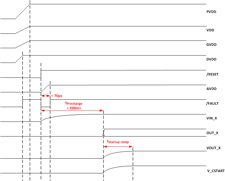
The TPA3255 does not require a power-up sequence, but it is recommended to hold RESET low for at least
250 ms after PVDD supply voltage is turned ON. The outputs of the H-bridges remain in a high-impedance state until the gate-drive supply voltage (GVDD_X) and VDD voltages are above the undervoltage protection (UVP) voltage threshold (see the Electrical Characteristics table of this data sheet). This allows an internal circuit to charge the external bootstrap capacitors by enabling a weak pulldown of the half-bridge output as well as initiating a controlled ramp up sequence of the output voltage.
When RESET is released to turn on TPA3255, FAULT signal will turn low and AVDD voltage regulator will be enabled. FAULT will stay low until AVDD reaches the undervoltage protection (UVP) voltage threshold (see the Electrical Characteristics table of this data sheet). After a precharge time to stabilize the DC voltage across the input AC coupling capacitors, the ramp up sequence starts.
11.3 Powering Down
The TPA3255 does not require a power-down sequence. The device remains fully operational as long as the gate-drive supply (GVDD_X) voltage and VDD voltage are above the undervoltage protection (UVP) voltage threshold (see the Electrical Characteristics table of this data sheet). Although not specifically required, it is a good practice to hold RESET low during power down, thus preventing audible artifacts including pops or clicks by initiating a controlled ramp down sequence of the output voltage.
11.4 Thermal Design
11.4.1 Thermal Performance
TPA3255 thermal performance is dependent on the design of the thermal system, which is the heatsink design and surrounding conditions including system enclosure (closed box with no air flow, or a fanned system etc.). As a result, the maximum continuous output power attainable will be influenced by the thermal design.
To mitigate thermal limitations in systems with the device operated at continuous high power it is advised to increase the cooling capability of the thermal system, or to operate the device in PBTL operation mode.
11.4.2 Thermal Performance with Continuous Output Power
It is recommended to operate TPA3255 below the OTW threshold. In most systems normal use conditions will safely keep the device temperature with margin to the OTW threshold. However in some systems and use cases the device tempertaure can run high, dependent on the actual output power, operating voltage, and thermal system. At high operating temperature some thermal limitations for continuous output power may occur at low audio frequencies due to increased heating of the output MOSFETs. Figure 33 shows maximum attainable continuous output power with a heatsink temperature of 75ºC and maximum 10% THD.
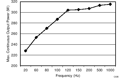 Figure 33. Maximum Continuous Output Power vs Frequency, BTL, 4Ω Load, Each Channel, TC = 75°C
11.4.3 Thermal Performance with Non-Continuous Output Power
As audio signals often have a peak to average ratio larger than one (average level below maximum peak output), the thermal performance for audio signals can be illustrated using burst signals with different burst ratios.
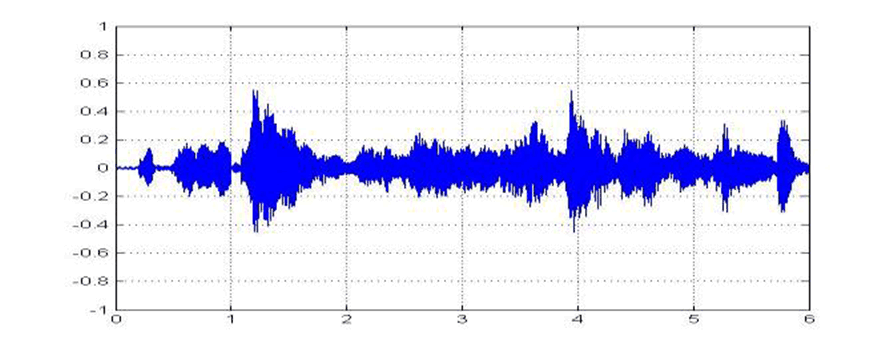 Figure 34. Example of audio signal
A burst signal is characterized by the high-level to low-level ratio as well as the duration of the high level and low level, e.g. a burst 1:4 stimuli is a single period of high level followed by 4 cycles of low level.
 Figure 35. Example of 1:4 Burst Signal
The following analysis of thermal performance for TPA3255 is made with the heatsink temperature controlled to 75°C.
The device is not thermally limited with 8-Ω load, but depending on the burst stimuli for operation at 75ºC heatsink temperature some thermal limitations may occur with a lower load impedance, depending on switching frequency and average to maximum power ratio. The figure below shows burst performance with a signal power ratio of 1:16 (low cycles power level 1/16 of the high cycles power level) and 1:8 .
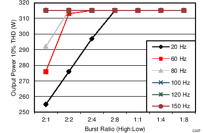 Figure 36. Maximum Burst Output Power vs Frequency, BTL, 4Ω Load, Each Channel, TC = 75°C, Power Ratio 1:16
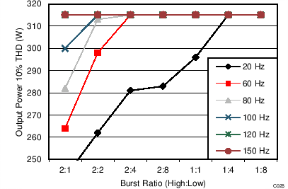 Figure 37. Maximum Burst Output Power vs Frequency, BTL, 4Ω Load, Each Channel, TC = 75°C, Power Ratio 1:8
