ZHCSFQ5A April 2016 – November 2016 TPA3244
PRODUCTION DATA.
- 1 特性
- 2 应用
- 3 说明
- 4 修订历史记录
- 5 Device Comparison Table
- 6 Pin Configuration and Functions
- 7 Specifications
- 8 Parameter Measurement Information
-
9 Detailed Description
- 9.1 Overview
- 9.2 Functional Block Diagrams
- 9.3 Feature Description
- 9.4
Device Functional Modes
- 9.4.1
Device Protection System
- 9.4.1.1 Overload and Short Circuit Current Protection
- 9.4.1.2 Signal Clipping and Pulse Injector
- 9.4.1.3 DC Speaker Protection
- 9.4.1.4 Pin-to-Pin Short Circuit Protection (PPSC)
- 9.4.1.5 Overtemperature Protection OTW and OTE
- 9.4.1.6 Undervoltage Protection (UVP) and Power-on Reset (POR)
- 9.4.1.7 Fault Handling
- 9.4.1.8 Device Reset
- 9.4.1
Device Protection System
-
10Application and Implementation
- 10.1 Application Information
- 10.2 Typical Applications
- 10.3 Typical Application, Differential (2N), PBTL (Outputs Paralleled after LC filter)
- 11Power Supply Recommendations
-
12Layout
- 12.1 Layout Guidelines
- 12.2
Layout Examples
- 12.2.1 BTL Application Printed Circuit Board Layout Example
- 12.2.2 SE Application Printed Circuit Board Layout Example
- 12.2.3 PBTL (Outputs Paralleled before LC filter) Application Printed Circuit Board Layout Example
- 12.2.4 PBTL (Outputs Paralleled after LC filter) Application Printed Circuit Board Layout Example
- 13器件和文档支持
- 14机械、封装和可订购信息
7 Specifications
7.1 Absolute Maximum Ratings
over operating free-air temperature range (unless otherwise noted) (1)| MIN | MAX | UNIT | ||
|---|---|---|---|---|
| Supply voltage | BST_X to GVDD_X(2) | –0.3 | 43 | V |
| VDD to GND | –0.3 | 13.2 | V | |
| GVDD_X to GND(2) | –0.3 | 13.2 | V | |
| PVDD_X to GND(2) | –0.3 | 43 | V | |
| DVDD to GND | –0.3 | 4.2 | V | |
| AVDD to GND | –0.3 | 8.5 | V | |
| VBG to GND | -0.3 | 4.2 | V | |
| Interface pins | OUT_X to GND(2) | –0.3 | 43 | V |
| BST_X to GND(2) | –0.3 | 55.5 | V | |
| OC_ADJ, M1, M2, OSC_IOP, OSC_IOM, FREQ_ADJ, C_START, to GND | –0.3 | 4.2 | V | |
| RESET, FAULT, CLIP_OTW, CLIP to GND | –0.3 | 4.2 | V | |
| INPUT_X to GND | –0.3 | 7 | V | |
| Continuous sink current, RESET, FAULT, CLIP_OTW, CLIP, RESET to GND | 9 | mA | ||
| TJ | Operating junction temperature range | 0 | 150 | °C |
| Tstg | Storage temperature range | –40 | 150 | °C |
7.2 ESD Ratings
| VALUE | UNIT | |||
|---|---|---|---|---|
| VESD | Electrostatic discharge | Human body model (HBM), per ANSI/ESDA/JEDEC JS-001, all pins (1) | ±1000 | V |
| Charged device model (CDM), per JEDEC specification JESD22-C101, all pins(2) | ±250 | V | ||
7.3 Recommended Operating Conditions
over operating free-air temperature range (unless otherwise noted)| MIN | TYP | MAX | UNIT | |||
|---|---|---|---|---|---|---|
| PVDD_x | Half-bridge supply | DC supply voltage | 12 | 30 | 31.5 | V |
| GVDD_x | Supply for logic regulators and gate-drive circuitry | DC supply voltage | 10.8 | 12 | 13.2 | V |
| VDD | Digital regulator supply voltage | DC supply voltage | 10.8 | 12 | 13.2 | V |
| RL(BTL) | Load impedance | Output filter inductance within recommended value range | 2.7 | 4 | Ω | |
| RL(SE) | 1.5 | 3 | ||||
| RL(PBTL) | 1.6 | 2 | ||||
| LOUT(BTL) | Output filter inductance | Minimum output inductance at IOC | 5 | μH | ||
| LOUT(SE) | 5 | |||||
| LOUT(PBTL) | 5 | |||||
| FPWM | PWM frame rate selectable for AM interference avoidance; 1% Resistor tolerance | Nominal | 430 | 450 | 470 | kHz |
| AM1 | 475 | 500 | 525 | |||
| AM2 | 575 | 600 | 625 | |||
| R(FREQ_ADJ) | PWM frame rate programming resistor | Nominal; Master mode | 29.7 | 30 | 30.3 | kΩ |
| AM1; Master mode | 19.8 | 20 | 20.2 | |||
| AM2; Master mode | 9.9 | 10 | 10.1 | |||
| CPVDD | PVDD close decoupling capacitors | 1.0 | μF | |||
| ROC | Over-current programming resistor | Resistor tolerance = 5% | 22 | 30 | kΩ | |
| ROC(LATCHED) | Over-current programming resistor | Resistor tolerance = 5% | 47 | 64 | kΩ | |
| V(FREQ_ADJ) | Voltage on FREQ_ADJ pin for slave mode operation | Slave mode | 3.3 | V | ||
| TJ | Junction temperature | 0 | 125 | °C | ||
7.4 Thermal Information
| THERMAL METRIC(1) | TPA3244 | UNIT | ||
|---|---|---|---|---|
| DDV 44-PINS HTSSOP | ||||
| JEDEC STANDARD 4 LAYER PCB | ||||
| RθJA | Junction-to-ambient thermal resistance | 23.0 | °C/W | |
| RθJC(top) | Junction-to-case (top) thermal resistance | 9.1 | °C/W | |
| RθJB | Junction-to-board thermal resistance | 3.9 | °C/W | |
| ψJT | Junction-to-top characterization parameter | 0.1 | °C/W | |
| ψJB | Junction-to-board characterization parameter | 3.9 | °C/W | |
| RθJC(bot) | Junction-to-case (bottom) thermal resistance | 0.3 | °C/W | |
7.5 Electrical Characteristics
PVDD_X = 30 V, GVDD_X = 12 V, VDD = 12 V, TA (Ambient temperature) = 25°C, fS = 450 kHz, unless otherwise specified.| PARAMETER | TEST CONDITIONS | MIN | TYP | MAX | UNIT | |
|---|---|---|---|---|---|---|
| INTERNAL VOLTAGE REGULATOR AND CURRENT CONSUMPTION | ||||||
| DVDD | Voltage regulator, only used as reference node | VDD = 12 V | 3 | 3.3 | 3.6 | V |
| AVDD | Voltage regulator, only used as reference node | VDD = 12 V | 7.8 | V | ||
| IVDD | VDD supply current | Operating, 50% duty cycle | 40 | mA | ||
| Idle, reset mode | 13 | |||||
| IGVDD_X | Gate-supply current per full-bridge | 50% duty cycle | 15 | mA | ||
| Reset mode | 2 | |||||
| IPVDD_X | PVDD idle current per full bridge | 50% duty cycle with 10µH Output Filter Inductors | 12.5 | mA | ||
| Reset mode, No switching | 1 | mA | ||||
| ANALOG INPUTS | ||||||
| RIN | Input resistance | 24 | kΩ | |||
| VIN | Maximum input voltage swing | 7 | V | |||
| IIN | Maximum input current | 1 | mA | |||
| G | Inverting voltage Gain | VOUT/VIN | 20 | dB | ||
| OSCILLATOR | ||||||
| fOSC(IO+) | Nominal, Master Mode | FPWM × 6 | 2.58 | 2.7 | 2.82 | MHz |
| AM1, Master Mode | 2.85 | 3 | 3.15 | |||
| AM2, Master Mode | 3.45 | 3.6 | 3.75 | |||
| VIH | High level input voltage | 1.86 | V | |||
| VIL | Low level input voltage | 1.45 | V | |||
| OUTPUT-STAGE MOSFETs | ||||||
| RDS(on) | Drain-to-source resistance, low side (LS) | TJ = 25°C, Includes metallization resistance, GVDD = 12 V |
65 | mΩ | ||
| Drain-to-source resistance, high side (HS) | 65 | mΩ | ||||
| I/O PROTECTION | ||||||
| Vuvp,VDD,GVDD | Undervoltage protection limit, GVDD_x and VDD | 9.5 | V | |||
| Vuvp,VDD, GVDD,hyst (1) | 0.6 | V | ||||
| Vuvp,PVDD | Undervoltage protection limit, PVDD_x | 10 | V | |||
| Vuvp,PVDD,hyst (1) | 0.6 | V | ||||
| OTW | Overtemperature warning, CLIP_OTW(1) | 115 | 125 | 135 | °C | |
| OTWhyst (1) | Temperature drop needed below OTW temperature for CLIP_OTW to be inactive after OTW event. | 25 | °C | |||
| OTE(1) | Overtemperature error | 145 | 155 | 165 | °C | |
| OTEhyst (1) | A reset needs to occur for FAULT to be released following an OTE event | 25 | °C | |||
| OTE-OTW(differential) (1) | OTE-OTW differential | 30 | °C | |||
| OLPC | Overload protection counter | fPWM = 450 kHz | 2.3 | ms | ||
| IOC | Overcurrent limit protection | Resistor – programmable, nominal peak current in 1Ω load, ROCP = 22 kΩ | 14 | A | ||
| IOC(LATCHED) | Overcurrent limit protection | Resistor – programmable, peak current in 1Ω load, ROCP = 47kΩ | 14 | A | ||
| IDCspkr | DC Speaker Protection Current Threshold | BTL current imbalance threshold | 1.5 | A | ||
| IOCT | Overcurrent response time | Time from switching transition to flip-state induced by overcurrent. | 150 | ns | ||
| IPD | Output pulldown current of each half | Connected when RESET is active to provide bootstrap charge. Not used in SE mode. | 3 | mA | ||
| STATIC DIGITAL SPECIFICATIONS | ||||||
| VIH | High level input voltage | M1, M2, OSC_IOP, OSC_IOM, RESET | 1.9 | V | ||
| VIL | Low level input voltage | 0.8 | V | |||
| Ilkg | Input leakage current | 100 | μA | |||
| OTW/SHUTDOWN (FAULT) | ||||||
| RINT_PU | Internal pullup resistance, CLIP_OTW to DVDD, FAULT to DVDD | 20 | 26 | 32 | kΩ | |
| VOH | High level output voltage | Internal pullup resistor | 3 | 3.3 | 3.6 | V |
| VOL | Low level output voltage | IO = 4 mA | 200 | 500 | mV | |
| Device fanout | CLIP_OTW, FAULT | No external pullup | 30 | devices | ||
7.6 Audio Characteristics (BTL)
PCB and system configuration are in accordance with recommended guidelines. Audio frequency = 1 kHz, PVDD_X = 30 V, GVDD_X = 12 V, RL = 8 Ω, fS = 450 kHz, ROC = 22 kΩ, TA = 25°C, Output Filter: LDEM = 10 μH, CDEM = 1 µF, mode = 00, AES17 + AUX-0025 measurement filters,unless otherwise noted.| PARAMETER | TEST CONDITIONS | MIN | TYP | MAX | UNIT | |
|---|---|---|---|---|---|---|
| PO | Power output per channel | RL = 8 Ω, 10% THD+N | 60 | W | ||
| RL = 4 Ω, 10% THD+N, Single Channel, 20 seconds duration(1) | 110 | |||||
| RL = 8 Ω, 1% THD+N | 50 | |||||
| RL = 4 Ω, 1% THD+N, 3 seconds Peak Power(1) | 90 | |||||
| RL = 4 Ω, 1% THD+N, Single Channel, 40 seconds Peak Power(1) | 90 | |||||
| THD+N | Total harmonic distortion + noise | 1 W | 0.005% | |||
| Vn | Output integrated noise | A-weighted, AES17 filter, Input Capacitor Grounded | 60 | μV | ||
| |VOS| | Output offset voltage | Inputs AC coupled to GND | 20 | 60 | mV | |
| SNR | Signal-to-noise ratio(2) | 111 | dB | |||
| DNR | Dynamic range | 111 | dB | |||
| Pidle | Power dissipation due to Idle losses (IPVDD_X) | PO = 0, 4 channels switching(3) | 0.38 | W | ||
7.7 Audio Characteristics (SE)
PCB and system configuration are in accordance with recommended guidelines. Audio frequency = 1 kHz, PVDD_X = 30 V, GVDD_X = 12 V, RL = 4 Ω, fS = 450 kHz, ROC = 22 kΩ, TA = 25°C, Output Filter: LDEM = 15 μH, CDEM = 1 µF, MODE = 11, AES17 + AUX-0025 measurement filters, unless otherwise noted.| PARAMETER | TEST CONDITIONS | MIN | TYP | MAX | UNIT | |
|---|---|---|---|---|---|---|
| PO | Power output per channel | RL = 4 Ω, 10% THD+N | 30 | W | ||
| RL = 3 Ω, 10% THD+N | 39 | |||||
| RL = 4 Ω, 1% THD+N | 25 | |||||
| RL = 3 Ω, 1% THD+N | 32 | |||||
| THD+N | Total harmonic distortion + noise | 1 W | 0.01% | |||
| Vn | Output integrated noise | A-weighted, AES17 filter, Input Capacitor Grounded | 100 | μV | ||
| SNR | Signal to noise ratio(1) | A-weighted | 100 | dB | ||
| DNR | Dynamic range | A-weighted | 101 | dB | ||
| Pidle | Power dissipation due to idle losses (IPVDD_X) | PO = 0, 4 channels switching(2) | 0.38 | W | ||
7.8 Audio Characteristics (PBTL)
PCB and system configuration are in accordance with recommended guidelines. Audio frequency = 1 kHz, PVDD_X = 30 V, GVDD_X = 12 V, RL = 4 Ω, fS = 450 kHz, ROC = 22 kΩ, TA = 25°C, Output Filter: LDEM = 10 μH, CDEM = 1 µF, MODE = 10, outputs paralleled before LC filter, AES17 + AUX-0025 measurement filters, unless otherwise noted.| PARAMETER | TEST CONDITIONS | MIN | TYP | MAX | UNIT | |
|---|---|---|---|---|---|---|
| PO | Power output per channel | RL = 4 Ω, 10% THD+N | 125 | W | ||
| RL = 3 Ω, 10% THD+N | 160 | |||||
| RL = 4 Ω, 1% THD+N | 100 | |||||
| RL = 3 Ω, 1% THD+N | 130 | |||||
| THD+N | Total harmonic distortion + noise | 1 W | 0.005% | |||
| Vn | Output integrated noise | A-weighted, AES17 filter, Input Capacitor Grounded | 55 | μV | ||
| SNR | Signal to noise ratio(1) | A-weighted | 112 | dB | ||
| DNR | Dynamic range | A-weighted | 112 | dB | ||
| Pidle | Power dissipation due to idle losses (IPVDD_X) | PO = 0, 4 channels switching(2) | 0.38 | W | ||
7.9 Typical Characteristics
7.9.1 BTL Configuration
All Measurements taken at audio frequency = 1 kHz, PVDD_X = 30 V, GVDD_X = 12 V, RL = 8 Ω, fS = 450 kHz, ROC = 22 kΩ, TA = 25°C, Output Filter: LDEM = 10 μH, CDEM = 1 µF, mode = 00, AES17 + AUX-0025 measurement filters,unless otherwise noted.
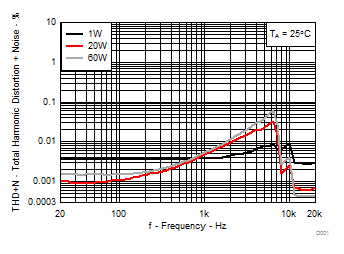
| RL = 4 Ω | P = 1W, 20W, 60W | TA = 25°C |
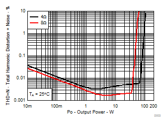
| RL =4 Ω, 8 Ω | TA = 25°C |
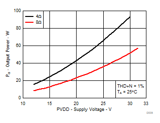
| RL = 4 Ω, 8 Ω | THD+N = 1% | TA = 25°C |
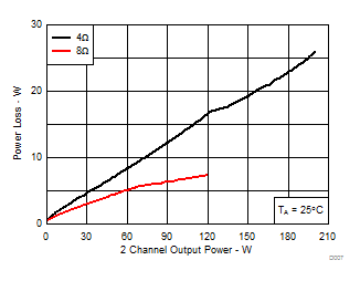
| RL = 4 Ω, 8 Ω | TA = 25°C | |
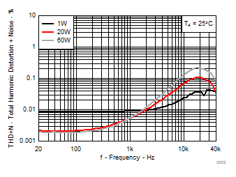
| RL = 4 Ω | P = 1W, 20W, 60W | TA = 25°C |
| AUX-0025 filter, 80 kHz analyzer BW | ||
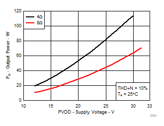
| RL = 4 Ω, 8 Ω | THD+N = 10% | TA = 25°C |
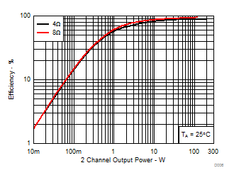
| RL = 4 Ω, 8 Ω | TA = 25°C |
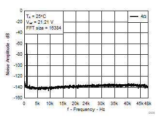
| 8 Ω, VREF = 25.46 V (1% Output power) | FFT = 16384 | |||
| AUX-0025 filter, 80 kHz analyzer BW | TA = 25°C | |||
7.9.2 SE Configuration
All Measurements taken at audio frequency = 1 kHz, PVDD_X = 30 V, GVDD_X = 12 V, RL = 4 Ω, fS = 450 kHz, ROC = 22 kΩ, TA = 25°C, Output Filter: LDEM = 15 μH, CDEM = 680 nF, MODE = 11, AES17 + AUX-0025 measurement filters, unless otherwise noted.
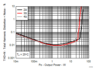
| RL = 2 Ω, 3Ω, 4Ω | TA = 25°C |
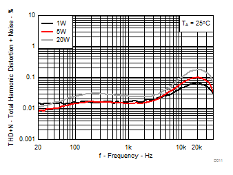
| RL = 4Ω | P = 1W, 5W, 20W | TA = 25°C |
| AUX-0025 filter, 80 kHz analyzer BW | ||
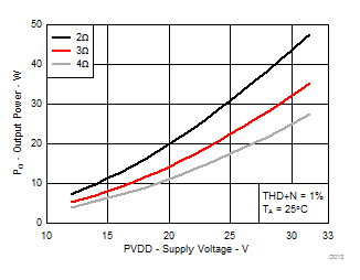
| RL = 2 Ω, 3Ω, 4Ω | THD+N = 1% | TA = 25°C |
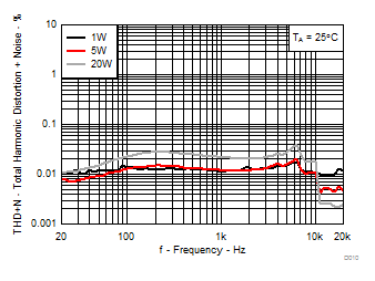
| RL = 4Ω | P = 1W, 5W, 20W | TA = 25°C |
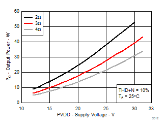
| RL = 2 Ω, 3Ω, 4Ω | THD+N = 10% | TA = 25°C |
7.9.3 PBTL Configuration
All Measurements taken at audio frequency = 1kHz, PVDD_X = 30 V, GVDD_X = 12 V, RL = 4Ω, fS = 450 kHz, ROC = 22 kΩ, TA = 25°C, Output Filter: LDEM = 10 μH, CDEM = 1 µF, MODE = 10, outputs paralleled before LC filter, AES17 + AUX-0025 measurement filters, unless otherwise noted.
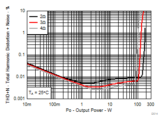
| RL = 2 Ω, 3Ω, 8Ω | TA = 25°C |
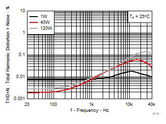
| RL = 2Ω | P = 1W, 40W, 120W | TA = 25°C |
| AUX-0025 filter, 80 kHz analyzer BW | ||
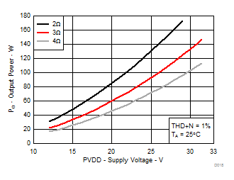
| RL = 2Ω, 3Ω, 4Ω | THD+N = 1% | TA = 25°C |
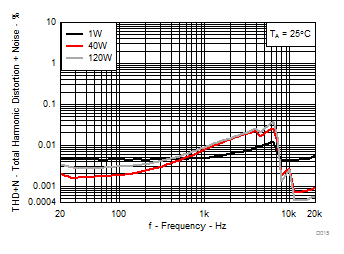
| RL = 2Ω | P = 1W, 40W, 120W | TA = 25°C |
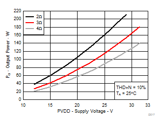
| RL = 2Ω, 3Ω, 4Ω | THD+N = 10% | TA = 25°C |