SPRS377F September 2008 – June 2014 TMS320C6745 , TMS320C6747
PRODUCTION DATA.
- 1TMS320C6745, TMS320C6747 Fixed- and Floating-Point Digital Signal Processor
- 2Revision History
-
3Device Overview
- 3.1 Device Characteristics
- 3.2 Device Compatibility
- 3.3 DSP Subsystem
- 3.4 Memory Map Summary
- 3.5 Pin Assignments
- 3.6
Terminal Functions
- 3.6.1 Device Reset and JTAG
- 3.6.2 High-Frequency Oscillator and PLL
- 3.6.3 Real-Time Clock and 32-kHz Oscillator
- 3.6.4 External Memory Interface A (ASYNC, SDRAM)
- 3.6.5 External Memory Interface B (only SDRAM)
- 3.6.6 Serial Peripheral Interface Modules (SPI0, SPI1)
- 3.6.7 Enhanced Capture/Auxiliary PWM Modules (eCAP0, eCAP1, eCAP2)
- 3.6.8 Enhanced Pulse Width Modulators (eHRPWM0, eHRPWM1, eHRPWM2)
- 3.6.9 Enhanced Quadrature Encoder Pulse Module (eQEP)
- 3.6.10 Boot
- 3.6.11 Universal Asynchronous Receiver/Transmitters (UART0, UART1, UART2)
- 3.6.12 Inter-Integrated Circuit Modules (I2C0, I2C1)
- 3.6.13 Timers
- 3.6.14 Universal Host-Port Interface (UHPI)
- 3.6.15 Multichannel Audio Serial Ports (McASP0, McASP1, McASP2)
- 3.6.16 Universal Serial Bus Modules (USB0, USB1)
- 3.6.17 Ethernet Media Access Controller (EMAC)
- 3.6.18 Multimedia Card/Secure Digital (MMC/SD)
- 3.6.19 Liquid Crystal Display Controller (LCD)
- 3.6.20 General Purpose Input Output (GPIO)
- 3.6.21 Reserved and No Connect
- 3.6.22 Supply and Ground
- 3.6.23 Unused USB0 (USB2.0) and USB1 (USB1.1) Pin Configurations
- 4Device Configuration
-
5Device Operating Conditions
- 5.1 Absolute Maximum Ratings Over Operating Case Temperature Range (Unless Otherwise Noted)
- 5.2 Handling Ratings
- 5.3 Recommended Operating Conditions
- 5.4 Notes on Recommended Power-On Hours (POH)
- 5.5 Electrical Characteristics Over Recommended Ranges of Supply Voltage and Operating Case Temperature (Unless Otherwise Noted)
-
6Peripheral Information and Electrical Specifications
- 6.1 Parameter Information
- 6.2 Recommended Clock and Control Signal Transition Behavior
- 6.3 Power Supplies
- 6.4 Reset
- 6.5 Crystal Oscillator or External Clock Input
- 6.6 Clock PLLs
- 6.7 Interrupts
- 6.8 General-Purpose Input/Output (GPIO)
- 6.9 EDMA
- 6.10 External Memory Interface A (EMIFA)
- 6.11 External Memory Interface B (EMIFB)
- 6.12 Memory Protection Units
- 6.13 MMC / SD / SDIO (MMCSD)
- 6.14 Ethernet Media Access Controller (EMAC)
- 6.15 Management Data Input/Output (MDIO)
- 6.16 Multichannel Audio Serial Ports (McASP0, McASP1, and McASP2)
- 6.17
Serial Peripheral Interface Ports (SPI0, SPI1)
- 6.17.1 SPI Peripheral Registers Description(s)
- 6.17.2
SPI Electrical Data/Timing
- 6.17.2.1
Serial Peripheral Interface (SPI) Timing
- Table 6-54 General Timing Requirements for SPI0 Master Modes
- Table 6-55 General Timing Requirements for SPI0 Slave Modes
- Table 6-56 Additional SPI0 Master Timings, 4-Pin Enable Option
- Table 6-57 Additional SPI0 Master Timings, 4-Pin Chip Select Option
- Table 6-58 Additional SPI0 Master Timings, 5-Pin Option
- Table 6-59 Additional SPI0 Slave Timings, 4-Pin Enable Option
- Table 6-60 Additional SPI0 Slave Timings, 4-Pin Chip Select Option
- Table 6-61 Additional SPI0 Slave Timings, 5-Pin Option
- Table 6-62 General Timing Requirements for SPI1 Master Modes
- Table 6-63 General Timing Requirements for SPI1 Slave Modes
- Table 6-64 Additional SPI1 Master Timings, 4-Pin Enable Option
- Table 6-65 Additional SPI1 Master Timings, 4-Pin Chip Select Option
- Table 6-66 Additional SPI1 Master Timings, 5-Pin Option
- Table 6-67 Additional SPI1 Slave Timings, 4-Pin Enable Option
- Table 6-68 Additional SPI1 Slave Timings, 4-Pin Chip Select Option
- Table 6-69 Additional SPI1 Slave Timings, 5-Pin Option
- 6.17.2.1
Serial Peripheral Interface (SPI) Timing
- 6.18 Enhanced Capture (eCAP) Peripheral
- 6.19 Enhanced Quadrature Encoder (eQEP) Peripheral
- 6.20 Enhanced High-Resolution Pulse-Width Modulator (eHRPWM)
- 6.21 LCD Controller
- 6.22 Timers
- 6.23 Inter-Integrated Circuit Serial Ports (I2C0, I2C1)
- 6.24 Universal Asynchronous Receiver/Transmitter (UART)
- 6.25 USB1 Host Controller Registers (USB1.1 OHCI)
- 6.26 USB0 OTG (USB2.0 OTG)
- 6.27 Host-Port Interface (UHPI)
- 6.28 Power and Sleep Controller (PSC)
- 6.29 Programmable Real-Time Unit Subsystem (PRUSS)
- 6.30 Emulation Logic
- 6.31 IEEE 1149.1 JTAG
- 6.32 Real Time Clock (RTC)
- 7Device and Documentation Support
- 8Mechanical Packaging and Orderable Information
3 Device Overview
3.1 Device Characteristics
Table 3-1 provides an overview of the C6745/6747 low power digital signal processor. The table shows significant features of the device, including the capacity of on-chip RAM, peripherals, and the package type with pin count.
Table 3-1 Characteristics of the C6745/C6747 Processor
| HARDWARE FEATURES | C6745 | C6747 | ||
|---|---|---|---|---|
| Peripherals Not all peripherals pins are available at the same time (for more detail, see the Device Configurations section). |
EMIFB | 16bit, up to 128MB SDRAM | 16/32bit, up to 256MB SDRAM | |
| EMIFA | Asynchronous (8-bit bus width) RAM, Flash, NOR, NAND | Asynchronous (8/16-bit bus width) RAM, Flash, 16bit up to 128MB SDRAM, NOR, NAND | ||
| Flash Card Interface | MMC and SD cards supported. | |||
| EDMA3 | 32 independent channels, 8 QDMA channels, 2 Transfer controllers | |||
| Timers | 2 64-Bit General Purpose (each configurable as 2 separate 32-bit timers, 1 configurable as Watch Dog) | |||
| UART | 3 (one with RTS and CTS flow control) | |||
| SPI | 2 (each with one hardware chip select) | |||
| I2C | 2 (both Master/Slave) | |||
| Multichannel Audio Serial Port [McASP] | 2 (each with transmit/receive, FIFO buffer, 16/9 serializers) | 3 (each with transmit/receive, FIFO buffer, 16/9 serializers) | ||
| 10/100 Ethernet MAC with Management Data I/O | 1 (RMII Interface) | |||
| eHRPWM | 6 Single Edge, 6 Dual Edge Symmetric, or 3 Dual Edge Asymmetric Outputs | |||
| eCAP | 3 32-bit capture inputs or 3 32-bit auxiliary PWM outputs | |||
| eQEP | 2 32-bit QEP channels with 4 inputs/channel | |||
| UHPI | - | 1 (16-bit multiplexed address/data) | ||
| USB 2.0 (USB0) | Full Speed Host Or Device with On-Chip PHY | High-Speed OTG Controller with on-chip OTG PHY | ||
| USB 1.1 (USB1) | - | Full-Speed OHCI (as host) with on-chip PHY | ||
| General-Purpose Input/Output Port | 8 banks of 16-bit | |||
| LCD Controller | - | 1 | ||
| RTC | - | 1 (32 KHz oscillator and seperate power trail. Provides time and date tracking and alarm capability.) | ||
| PRU Subsystem (PRUSS) | 2 Programmable PRU Cores | |||
| On-Chip Memory | Size (Bytes) | 320 KB RAM | 448 KB RAM | |
| Organization | DSP
32KB L1 Program (L1P)/Cache (up to 32KB) 32KB L1 Data (L1D)/Cache (up to 32KB) 256KB Unified Mapped RAM/Cache (L2) DSP Memories can be made accessible to EDMA3, and other peripherals. |
|||
| - | ADDITIONAL MEMORY
128KB RAM |
|||
| C674x CPU ID + CPU Rev ID | Control Status Register (CSR.[31:16]) | 0x1400 | ||
| C674x Megamodule Revision | Revision ID Register (MM_REVID[15:0]) | 0x0000 | ||
| JTAG BSDL_ID | DEVIDR0 register | 0x0B7D F02F (Silicon Revision 1.0) 0x8B7D F02F (Silicon Revision 1.1) 0x9B7D F02F (Silicon Revisions 3.0, 2.1, and 2.0) |
||
| CPU Frequency | MHz | 674x DSP at 375 MHz(1.2V) or 456 MHz (1.3V) | ||
| Voltage | Core (V) | 1.2V / 1.3V | ||
| I/O (V) | 3.3 V | |||
| Package | 24 mm x 24 mm, 176-Pin, 0.5 mm pitch, TQFP (PTP) | 17 mm x 17 mm, 256-Ball 1 mm pitch, PBGA (ZKB) | ||
| Product Status(1) | Product Preview (PP), Advance Information (AI), or Production Data (PD) |
375 MHz Versions -PD 456 MHz Version - PD |
||
3.2 Device Compatibility
The C674x DSP core is code-compatible with the C6000™ DSP platform and supports features of both the C64x+ and C67x+ DSP families.
3.3 DSP Subsystem
The DSP Subsystem includes the following features:
- C674x DSP CPU
- 32KB L1 Program (L1P)/Cache (up to 32KB)
- 32KB L1 Data (L1D)/Cache (up to 32KB)
- 256KB Unified Mapped RAM/Cache (L2)
- Boot ROM (cannot be used for application code)
- Little endian
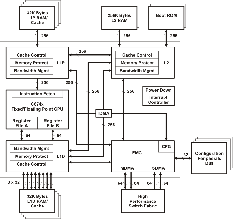 Figure 3-1 C674x Megamodule Block Diagram
3.3.1 C674x DSP CPU Description
The C674x Central Processing Unit (CPU) consists of eight functional units, two register files, and two data paths as shown in Figure 3-2. The two general-purpose register files (A and B) each contain 32 32-bit registers for a total of 64 registers. The general-purpose registers can be used for data or can be data address pointers. The data types supported include packed 8-bit data, packed 16-bit data, 32-bit data, 40-bit data, and 64-bit data. Values larger than 32 bits, such as 40-bit-long or 64-bit-long values are stored in register pairs, with the 32 LSBs of data placed in an even register and the remaining 8 or 32 MSBs in the next upper register (which is always an odd-numbered register).
The eight functional units (.M1, .L1, .D1, .S1, .M2, .L2, .D2, and .S2) are each capable of executing one instruction every clock cycle. The .M functional units perform all multiply operations. The .S and .L units perform a general set of arithmetic, logical, and branch functions. The .D units primarily load data from memory to the register file and store results from the register file into memory.
The C674x CPU combines the performance of the C64x+ core with the floating-point capabilities of the C67x+ core.
Each C674x .M unit can perform one of the following each clock cycle: one 32 x 32 bit multiply, one 16 x 32 bit multiply, two 16 x 16 bit multiplies, two 16 x 32 bit multiplies, two 16 x 16 bit multiplies with add/subtract capabilities, four 8 x 8 bit multiplies, four 8 x 8 bit multiplies with add operations, and four 16 x 16 multiplies with add/subtract capabilities (including a complex multiply). There is also support for Galois field multiplication for 8-bit and 32-bit data. Many communications algorithms such as FFTs and modems require complex multiplication. The complex multiply (CMPY) instruction takes four 16-bit inputs and produces a 32-bit real and a 32-bit imaginary output. There are also complex multiplies with rounding capability that produces one 32-bit packed output that contain 16-bit real and 16-bit imaginary values. The 32 x 32 bit multiply instructions provide the extended precision necessary for high-precision algorithms on a variety of signed and unsigned 32-bit data types.
The .L Unit (or Arithmetic Logic Unit) now incorporates the ability to do parallel add/subtract operations on a pair of common inputs. Versions of this instruction exist to work on 32-bit data or on pairs of 16-bit data performing dual 16-bit add and subtracts in parallel. There are also saturated forms of these instructions.
The C674x core enhances the .S unit in several ways. On the previous cores, dual 16-bit MIN2 and MAX2 comparisons were only available on the .L units. On the C674x core they are also available on the .S unit which increases the performance of algorithms that do searching and sorting. Finally, to increase data packing and unpacking throughput, the .S unit allows sustained high performance for the quad 8-bit/16-bit and dual 16-bit instructions. Unpack instructions prepare 8-bit data for parallel 16-bit operations. Pack instructions return parallel results to output precision including saturation support.
Other new features include:
- SPLOOP - A small instruction buffer in the CPU that aids in creation of software pipelining loops where multiple iterations of a loop are executed in parallel. The SPLOOP buffer reduces the code size associated with software pipelining. Furthermore, loops in the SPLOOP buffer are fully interruptible.
- Compact Instructions - The native instruction size for the C6000™ devices is 32 bits. Many common instructions such as MPY, AND, OR, ADD, and SUB can be expressed as 16 bits if the C674x compiler can restrict the code to use certain registers in the register file. This compression is performed by the code generation tools.
- Instruction Set Enhancement - As noted above, there are new instructions such as 32-bit multiplications, complex multiplications, packing, sorting, bit manipulation, and 32-bit Galois field multiplication.
- Exceptions Handling - Intended to aid the programmer in isolating bugs. The C674x CPU is able to detect and respond to exceptions, both from internally detected sources (such as illegal op-codes) and from system events (such as a watchdog time expiration).
- Privilege - Defines user and supervisor modes of operation, allowing the operating system to give a basic level of protection to sensitive resources. Local memory is divided into multiple pages, each with read, write, and execute permissions.
- Time-Stamp Counter - Primarily targeted for Real-Time Operating System (RTOS) robustness, a free-running time-stamp counter is implemented in the CPU which is not sensitive to system stalls.
For more details on the C674x CPU and its enhancements over the C64x architecture, see the following documents:
- TMS320C64x/C64x+ DSP CPU and Instruction Set Reference Guide (SPRU732)
- TMS320C64x Technical Overview (SPRU395)
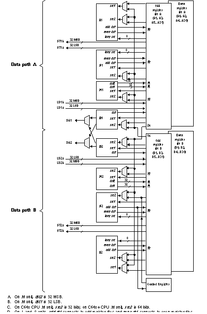 Figure 3-2 TMS320C674x CPU (DSP Core) Data Paths
3.3.2 DSP Memory Mapping
The DSP memory map is shown in Section 3.4.
3.3.2.1 External Memories
The DSP has access to the following External memories:
- Asynchronous EMIF / SDRAM / NAND / NOR Flash (EMIFA)
- SDRAM (EMIFB)
3.3.2.2 DSP Internal Memories
The DSP has access to the following DSP memories:
- L2 RAM
- L1P RAM
- L1D RAM
3.3.2.3 C674x CPU
The C674x core uses a two-level cache-based architecture. The Level 1 Program cache (L1P) is 32 KB direct mapped cache and the Level 1 Data cache (L1D) is 32 KB 2-way set associated cache. The Level 2 memory/cache (L2) consists of a 256 KB memory space that is shared between program and data space. L2 memory can be configured as mapped memory, cache, or a combination of both.
Table 3-2 shows a memory map of the C674x CPU cache registers for the device.
Table 3-2 C674x Cache Registers
| BYTE ADDRESS | ACRONYM | REGISTER DESCRIPTION |
|---|---|---|
| 0x0184 0000 | L2CFG | L2 Cache configuration register (See the Technical Reference Manual SPRUH91 for the reset configuration) |
| 0x0184 0020 | L1PCFG | L1P Size Cache configuration register (See the Technical Reference Manual SPRUH91 for the reset configuration) |
| 0x0184 0024 | L1PCC | L1P Freeze Mode Cache configuration register |
| 0x0184 0040 | L1DCFG | L1D Size Cache configuration register (See the Technical Reference Manual SPRUH91 for the reset configuration) |
| 0x0184 0044 | L1DCC | L1D Freeze Mode Cache configuration register |
| 0x0184 0048 - 0x0184 0FFC | - | Reserved |
| 0x0184 1000 | EDMAWEIGHT | L2 EDMA access control register |
| 0x0184 1004 - 0x0184 1FFC | - | Reserved |
| 0x0184 2000 | L2ALLOC0 | L2 allocation register 0 |
| 0x0184 2004 | L2ALLOC1 | L2 allocation register 1 |
| 0x0184 2008 | L2ALLOC2 | L2 allocation register 2 |
| 0x0184 200C | L2ALLOC3 | L2 allocation register 3 |
| 0x0184 2010 - 0x0184 3FFF | - | Reserved |
| 0x0184 4000 | L2WBAR | L2 writeback base address register |
| 0x0184 4004 | L2WWC | L2 writeback word count register |
| 0x0184 4010 | L2WIBAR | L2 writeback invalidate base address register |
| 0x0184 4014 | L2WIWC | L2 writeback invalidate word count register |
| 0x0184 4018 | L2IBAR | L2 invalidate base address register |
| 0x0184 401C | L2IWC | L2 invalidate word count register |
| 0x0184 4020 | L1PIBAR | L1P invalidate base address register |
| 0x0184 4024 | L1PIWC | L1P invalidate word count register |
| 0x0184 4030 | L1DWIBAR | L1D writeback invalidate base address register |
| 0x0184 4034 | L1DWIWC | L1D writeback invalidate word count register |
| 0x0184 4038 | - | Reserved |
| 0x0184 4040 | L1DWBAR | L1D writeback base address register |
| 0x0184 4044 | L1DWWC | L1D writeback word count register |
| 0x0184 4048 | L1DIBAR | L1D invalidate base address register |
| 0x0184 404C | L1DIWC | L1D invalidate word count register |
| 0x0184 4050 - 0x0184 4FFF | - | Reserved |
| 0x0184 5000 | L2WB | L2 writeback all register |
| 0x0184 5004 | L2WBINV | L2 writeback invalidate all register |
| 0x0184 5008 | L2INV | L2 Global Invalidate without writeback |
| 0x0184 500C - 0x0184 5027 | - | Reserved |
| 0x0184 5028 | L1PINV | L1P Global Invalidate |
| 0x0184 502C - 0x0184 5039 | - | Reserved |
| 0x0184 5040 | L1DWB | L1D Global Writeback |
| 0x0184 5044 | L1DWBINV | L1D Global Writeback with Invalidate |
| 0x0184 5048 | L1DINV | L1D Global Invalidate without writeback |
| 0x0184 8000 – 0x0184 80FF | MAR0 - MAR63 | Reserved 0x0000 0000 – 0x3FFF FFFF |
| 0x0184 8100 – 0x0184 817F | MAR64 – MAR95 | Memory Attribute Registers for EMIFA SDRAM Data (CS0) 0x4000 0000 – 0x5FFF FFFF |
| 0x0184 8180 – 0x0184 8187 | MAR96 - MAR97 | Memory Attribute Registers for EMIFA Async Data (CS2) 0x6000 0000 – 0x61FF FFFF |
| 0x0184 8188 – 0x0184 818F | MAR98 – MAR99 | Memory Attribute Registers for EMIFA Async Data (CS3) 0x6200 0000 – 0x63FF FFFF |
| 0x0184 8190 – 0x0184 8197 | MAR100 – MAR101 | Memory Attribute Registers for EMIFA Async Data (CS4) 0x6400 0000 – 0x65FF FFFF |
| 0x0184 8198 – 0x0184 819F | MAR102 – MAR103 | Memory Attribute Registers for EMIFA Async Data (CS5) 0x6600 0000 – 0x67FF FFFF |
| 0x0184 81A0 – 0x0184 81FF | MAR104 – MAR127 | Reserved 0x6800 0000 – 0x7FFF FFFF |
| 0x0184 8200 | MAR128 | Memory Attribute Register for Shared RAM 0x8000 0000 – 0x8001 FFFF |
| Reserved 0x8002 0000 – 0x81FF FFFF | ||
| 0x0184 8204 – 0x0184 82FF | MAR129 – MAR191 | Reserved 0x8200 0000 – 0xBFFF FFFF |
| 0x0184 8300 – 0x0184 837F | MAR192 – MAR223 | Memory Attribute Registers for EMIFB SDRAM Data (CS0) 0xC000 0000 – 0xDFFF FFFF |
| 0x0184 8380 – 0x0184 83FF | MAR224 – MAR255 | Reserved 0xE000 0000 – 0xFFFF FFFF |
Table 3-3 C674x L1/L2 Memory Protection Registers
| BYTE ADDRESS | ACRONYM | REGISTER DESCRIPTION |
|---|---|---|
| 0x0184 A000 | L2MPFAR | L2 memory protection fault address register |
| 0x0184 A004 | L2MPFSR | L2 memory protection fault status register |
| 0x0184 A008 | L2MPFCR | L2 memory protection fault command register |
| 0x0184 A00C - 0x0184 A0FF | - | Reserved |
| 0x0184 A100 | L2MPLK0 | L2 memory protection lock key bits [31:0] |
| 0x0184 A104 | L2MPLK1 | L2 memory protection lock key bits [63:32] |
| 0x0184 A108 | L2MPLK2 | L2 memory protection lock key bits [95:64] |
| 0x0184 A10C | L2MPLK3 | L2 memory protection lock key bits [127:96] |
| 0x0184 A110 | L2MPLKCMD | L2 memory protection lock key command register |
| 0x0184 A114 | L2MPLKSTAT | L2 memory protection lock key status register |
| 0x0184 A118 - 0x0184 A1FF | - | Reserved |
| 0x0184 A200 | L2MPPA0 | L2 memory protection page attribute register 0 (controls memory address 0x0080 0000 - 0x0080 1FFF) |
| 0x0184 A204 | L2MPPA1 | L2 memory protection page attribute register 1 (controls memory address 0x0080 2000 - 0x0080 3FFF) |
| 0x0184 A208 | L2MPPA2 | L2 memory protection page attribute register 2 (controls memory address 0x0080 4000 - 0x0080 5FFF) |
| 0x0184 A20C | L2MPPA3 | L2 memory protection page attribute register 3 (controls memory address 0x0080 6000 - 0x0080 7FFF) |
| 0x0184 A210 | L2MPPA4 | L2 memory protection page attribute register 4 (controls memory address 0x0080 8000 - 0x0080 9FFF) |
| 0x0184 A214 | L2MPPA5 | L2 memory protection page attribute register 5 (controls memory address 0x0080 A000 - 0x0080 BFFF) |
| 0x0184 A218 | L2MPPA6 | L2 memory protection page attribute register 6 (controls memory address 0x0080 C000 - 0x0080 DFFF) |
| 0x0184 A21C | L2MPPA7 | L2 memory protection page attribute register 7 (controls memory address 0x0080 E000 - 0x0080 FFFF) |
| 0x0184 A220 | L2MPPA8 | L2 memory protection page attribute register 8 (controls memory address 0x0081 0000 - 0x0081 1FFF) |
| 0x0184 A224 | L2MPPA9 | L2 memory protection page attribute register 9 (controls memory address 0x0081 2000 - 0x0081 3FFF) |
| 0x0184 A228 | L2MPPA10 | L2 memory protection page attribute register 10 (controls memory address 0x0081 4000 - 0x0081 5FFF) |
| 0x0184 A22C | L2MPPA11 | L2 memory protection page attribute register 11 (controls memory address 0x0081 6000 - 0x0081 7FFF) |
| 0x0184 A230 | L2MPPA12 | L2 memory protection page attribute register 12 (controls memory address 0x0081 8000 - 0x0081 9FFF) |
| 0x0184 A234 | L2MPPA13 | L2 memory protection page attribute register 13 (controls memory address 0x0081 A000 - 0x0081 BFFF) |
| 0x0184 A238 | L2MPPA14 | L2 memory protection page attribute register 14 (controls memory address 0x0081 C000 - 0x0081 DFFF) |
| 0x0184 A23C | L2MPPA15 | L2 memory protection page attribute register 15 (controls memory address 0x0081 E000 - 0x0081 FFFF) |
| 0x0184 A240 | L2MPPA16 | L2 memory protection page attribute register 16 (controls memory address 0x0082 0000 - 0x0082 1FFF) |
| 0x0184 A244 | L2MPPA17 | L2 memory protection page attribute register 17 (controls memory address 0x0082 2000 - 0x0082 3FFF) |
| 0x0184 A248 | L2MPPA18 | L2 memory protection page attribute register 18 (controls memory address 0x0082 4000 - 0x0082 5FFF) |
| 0x0184 A24C | L2MPPA19 | L2 memory protection page attribute register 19 (controls memory address 0x0082 6000 - 0x0082 7FFF) |
| 0x0184 A250 | L2MPPA20 | L2 memory protection page attribute register 20 (controls memory address 0x0082 8000 - 0x0082 9FFF) |
| 0x0184 A254 | L2MPPA21 | L2 memory protection page attribute register 21 (controls memory address 0x0082 A000 - 0x0082 BFFF) |
| 0x0184 A258 | L2MPPA22 | L2 memory protection page attribute register 22 (controls memory address 0x0082 C000 - 0x0082 DFFF) |
| 0x0184 A25C | L2MPPA23 | L2 memory protection page attribute register 23 (controls memory address 0x0082 E000 - 0x0082 FFFF) |
| 0x0184 A260 | L2MPPA24 | L2 memory protection page attribute register 24 (controls memory address 0x0083 0000 - 0x0083 1FFF) |
| 0x0184 A264 | L2MPPA25 | L2 memory protection page attribute register 25 (controls memory address 0x0083 2000 - 0x0083 3FFF) |
| 0x0184 A268 | L2MPPA26 | L2 memory protection page attribute register 26 (controls memory address 0x0083 4000 - 0x0083 5FFF) |
| 0x0184 A26C | L2MPPA27 | L2 memory protection page attribute register 27 (controls memory address 0x0083 6000 - 0x0083 7FFF) |
| 0x0184 A270 | L2MPPA28 | L2 memory protection page attribute register 28 (controls memory address 0x0083 8000 - 0x0083 9FFF) |
| 0x0184 A274 | L2MPPA29 | L2 memory protection page attribute register 29 (controls memory address 0x0083 A000 - 0x0083 BFFF) |
| 0x0184 A278 | L2MPPA30 | L2 memory protection page attribute register 30 (controls memory address 0x0083 C000 - 0x0083 DFFF) |
| 0x0184 A27C | L2MPPA31 | L2 memory protection page attribute register 31 (controls memory address 0x0083 E000 - 0x0083 FFFF) |
| 0x0184 A280 | L2MPPA32 | L2 memory protection page attribute register 32 (controls memory address 0x0070 0000 - 0x0070 7FFF) |
| 0x0184 A284 | L2MPPA33 | L2 memory protection page attribute register 33 (controls memory address 0x0070 8000 - 0x0070 FFFF) |
| 0x0184 A288 | L2MPPA34 | L2 memory protection page attribute register 34 (controls memory address 0x0071 0000 - 0x0071 7FFF) |
| 0x0184 A28C | L2MPPA35 | L2 memory protection page attribute register 35 (controls memory address 0x0071 8000 - 0x0071 FFFF) |
| 0x0184 A290 | L2MPPA36 | L2 memory protection page attribute register 36 (controls memory address 0x0072 0000 - 0x0072 7FFF) |
| 0x0184 A294 | L2MPPA37 | L2 memory protection page attribute register 37 (controls memory address 0x0072 8000 - 0x0072 FFFF) |
| 0x0184 A298 | L2MPPA38 | L2 memory protection page attribute register 38 (controls memory address 0x0073 0000 - 0x0073 7FFF) |
| 0x0184 A29C | L2MPPA39 | L2 memory protection page attribute register 39 (controls memory address 0x0073 8000 - 0x0073 FFFF) |
| 0x0184 A2A0 | L2MPPA40 | L2 memory protection page attribute register 40 (controls memory address 0x0074 0000 - 0x0074 7FFF) |
| 0x0184 A2A4 | L2MPPA41 | L2 memory protection page attribute register 41 (controls memory address 0x0074 8000 - 0x0074 FFFF) |
| 0x0184 A2A8 | L2MPPA42 | L2 memory protection page attribute register 42 (controls memory address 0x0075 0000 - 0x0075 7FFF) |
| 0x0184 A2AC | L2MPPA43 | L2 memory protection page attribute register 43 (controls memory address 0x0075 8000 - 0x0075 FFFF) |
| 0x0184 A2B0 | L2MPPA44 | L2 memory protection page attribute register 44 (controls memory address 0x0076 0000 - 0x0076 7FFF) |
| 0x0184 A2B4 | L2MPPA45 | L2 memory protection page attribute register 45 (controls memory address 0x0076 8000 - 0x0076 FFFF) |
| 0x0184 A2B8 | L2MPPA46 | L2 memory protection page attribute register 46 (controls memory address 0x0077 0000 - 0x0077 7FFF) |
| 0x0184 A2BC | L2MPPA47 | L2 memory protection page attribute register 47 (controls memory address 0x0077 8000 - 0x0077 FFFF) |
| 0x0184 A2C0 | L2MPPA48 | L2 memory protection page attribute register 48 (controls memory address 0x0078 0000 - 0x0078 7FFF) |
| 0x0184 A2C4 | L2MPPA49 | L2 memory protection page attribute register 49 (controls memory address 0x0078 8000 - 0x0078 FFFF) |
| 0x0184 A2C8 | L2MPPA50 | L2 memory protection page attribute register 50 (controls memory address 0x0079 0000 - 0x0079 7FFF) |
| 0x0184 A2CC | L2MPPA51 | L2 memory protection page attribute register 51 (controls memory address 0x0079 8000 - 0x0079 FFFF) |
| 0x0184 A2D0 | L2MPPA52 | L2 memory protection page attribute register 52 (controls memory address 0x007A 0000 - 0x007A 7FFF) |
| 0x0184 A2D4 | L2MPPA53 | L2 memory protection page attribute register 53 (controls memory address 0x007A 8000 - 0x007A FFFF) |
| 0x0184 A2D8 | L2MPPA54 | L2 memory protection page attribute register 54 (controls memory address 0x007B 0000 - 0x007B 7FFF) |
| 0x0184 A2DC | L2MPPA55 | L2 memory protection page attribute register 55 (controls memory address 0x007B 8000 - 0x007B FFFF) |
| 0x0184 A2E0 | L2MPPA56 | L2 memory protection page attribute register 56 (controls memory address 0x007C 0000 - 0x007C 7FFF) |
| 0x0184 A2E4 | L2MPPA57 | L2 memory protection page attribute register 57 (controls memory address 0x007C 8000 - 0x007C FFFF) |
| 0x0184 A2E8 | L2MPPA58 | L2 memory protection page attribute register 58 (controls memory address 0x007D 0000 - 0x007D 7FFF) |
| 0x0184 A2EC | L2MPPA59 | L2 memory protection page attribute register 59 (controls memory address 0x007D 8000 - 0x007D FFFF) |
| 0x0184 A2F0 | L2MPPA60 | L2 memory protection page attribute register 60 (controls memory address 0x007E 0000 - 0x007E 7FFF) |
| 0x0184 A2F4 | L2MPPA61 | L2 memory protection page attribute register 61 (controls memory address 0x007E 8000 - 0x007E FFFF) |
| 0x0184 A2F8 | L2MPPA62 | L2 memory protection page attribute register 62 (controls memory address 0x007F 0000 - 0x007F 7FFF) |
| 0x0184 A2FC | L2MPPA63 | L2 memory protection page attribute register 63 (controls memory address 0x007F 8000 - 0x007F FFFF) |
| 0x0184 A300 - 0x0184 A3FF | - | Reserved |
| 0x0184 A400 | L1PMPFAR | L1P memory protection fault address register |
| 0x0184 A404 | L1PMPFSR | L1P memory protection fault status register |
| 0x0184 A408 | L1PMPFCR | L1P memory protection fault command register |
| 0x0184 A40C - 0x0184 A4FF | - | Reserved |
| 0x0184 A500 | L1PMPLK0 | L1P memory protection lock key bits [31:0] |
| 0x0184 A504 | L1PMPLK1 | L1P memory protection lock key bits [63:32] |
| 0x0184 A508 | L1PMPLK2 | L1P memory protection lock key bits [95:64] |
| 0x0184 A50C | L1PMPLK3 | L1P memory protection lock key bits [127:96] |
| 0x0184 A510 | L1PMPLKCMD | L1P memory protection lock key command register |
| 0x0184 A514 | L1PMPLKSTAT | L1P memory protection lock key status register |
| 0x0184 A518 - 0x0184 A5FF | - | Reserved |
| 0x0184 A600 - 0x0184 A63F | - | Reserved (1) |
| 0x0184 A640 | L1PMPPA16 | L1P memory protection page attribute register 16 (controls memory address 0x00E0 0000 - 0x00E0 07FF) |
| 0x0184 A644 | L1PMPPA17 | L1P memory protection page attribute register 17 (controls memory address 0x00E0 0800 - 0x00E0 0FFF) |
| 0x0184 A648 | L1PMPPA18 | L1P memory protection page attribute register 18 (controls memory address 0x00E0 1000 - 0x00E0 17FF) |
| 0x0184 A64C | L1PMPPA19 | L1P memory protection page attribute register 19 (controls memory address 0x00E0 1800 - 0x00E0 1FFF) |
| 0x0184 A650 | L1PMPPA20 | L1P memory protection page attribute register 20 (controls memory address 0x00E0 2000 - 0x00E0 27FF) |
| 0x0184 A654 | L1PMPPA21 | L1P memory protection page attribute register 21 (controls memory address 0x00E0 2800 - 0x00E0 2FFF) |
| 0x0184 A658 | L1PMPPA22 | L1P memory protection page attribute register 22 (controls memory address 0x00E0 3000 - 0x00E0 37FF) |
| 0x0184 A65C | L1PMPPA23 | L1P memory protection page attribute register 23 (controls memory address 0x00E0 3800 - 0x00E0 3FFF) |
| 0x0184 A660 | L1PMPPA24 | L1P memory protection page attribute register 24 (controls memory address 0x00E0 4000 - 0x00E0 47FF) |
| 0x0184 A664 | L1PMPPA25 | L1P memory protection page attribute register 25 (controls memory address 0x00E0 4800 - 0x00E0 4FFF) |
| 0x0184 A668 | L1PMPPA26 | L1P memory protection page attribute register 26 (controls memory address 0x00E0 5000 - 0x00E0 57FF) |
| 0x0184 A66C | L1PMPPA27 | L1P memory protection page attribute register 27 (controls memory address 0x00E0 5800 - 0x00E0 5FFF) |
| 0x0184 A670 | L1PMPPA28 | L1P memory protection page attribute register 28 (controls memory address 0x00E0 6000 - 0x00E0 67FF) |
| 0x0184 A674 | L1PMPPA29 | L1P memory protection page attribute register 29 (controls memory address 0x00E0 6800 - 0x00E0 6FFF) |
| 0x0184 A678 | L1PMPPA30 | L1P memory protection page attribute register 30 (controls memory address 0x00E0 7000 - 0x00E0 77FF) |
| 0x0184 A67C | L1PMPPA31 | L1P memory protection page attribute register 31 (controls memory address 0x00E0 7800 - 0x00E0 7FFF) |
| 0x0184 A67F – 0x0184 ABFF | - | Reserved |
| 0x0184 AC00 | L1DMPFAR | L1D memory protection fault address register |
| 0x0184 AC04 | L1DMPFSR | L1D memory protection fault status register |
| 0x0184 AC08 | L1DMPFCR | L1D memory protection fault command register |
| 0x0184 AC0C - 0x0184 ACFF | - | Reserved |
| 0x0184 AD00 | L1DMPLK0 | L1D memory protection lock key bits [31:0] |
| 0x0184 AD04 | L1DMPLK1 | L1D memory protection lock key bits [63:32] |
| 0x0184 AD08 | L1DMPLK2 | L1D memory protection lock key bits [95:64] |
| 0x0184 AD0C | L1DMPLK3 | L1D memory protection lock key bits [127:96] |
| 0x0184 AD10 | L1DMPLKCMD | L1D memory protection lock key command register |
| 0x0184 AD14 | L1DMPLKSTAT | L1D memory protection lock key status register |
| 0x0184 AD18 - 0x0184 ADFF | - | Reserved |
| 0x0184 AE00 - 0x0184 AE3F | - | Reserved (2) |
| 0x0184 AE40 | L1DMPPA16 | L1D memory protection page attribute register 16 (controls memory address 0x00F0 0000 - 0x00F0 07FF) |
| 0x0184 AE44 | L1DMPPA17 | L1D memory protection page attribute register 17 (controls memory address 0x00F0 0800 - 0x00F0 0FFF) |
| 0x0184 AE48 | L1DMPPA18 | L1D memory protection page attribute register 18 (controls memory address 0x00F0 1000 - 0x00F0 17FF) |
| 0x0184 AE4C | L1DMPPA19 | L1D memory protection page attribute register 19 (controls memory address 0x00F0 1800 - 0x00F0 1FFF) |
| 0x0184 AE50 | L1DMPPA20 | L1D memory protection page attribute register 20 (controls memory address 0x00F0 2000 - 0x00F0 27FF) |
| 0x0184 AE54 | L1DMPPA21 | L1D memory protection page attribute register 21 (controls memory address 0x00F0 2800 - 0x00F0 2FFF) |
| 0x0184 AE58 | L1DMPPA22 | L1D memory protection page attribute register 22 (controls memory address 0x00F0 3000 - 0x00F0 37FF) |
| 0x0184 AE5C | L1DMPPA23 | L1D memory protection page attribute register 23 (controls memory address 0x00F0 3800 - 0x00F0 3FFF) |
| 0x0184 AE60 | L1DMPPA24 | L1D memory protection page attribute register 24 (controls memory address 0x00F0 4000 - 0x00F0 47FF) |
| 0x0184 AE64 | L1DMPPA25 | L1D memory protection page attribute register 25 (controls memory address 0x00F0 4800 - 0x00F0 4FFF) |
| 0x0184 AE68 | L1DMPPA26 | L1D memory protection page attribute register 26 (controls memory address 0x00F0 5000 - 0x00F0 57FF) |
| 0x0184 AE6C | L1DMPPA27 | L1D memory protection page attribute register 27 (controls memory address 0x00F0 5800 - 0x00F0 5FFF) |
| 0x0184 AE70 | L1DMPPA28 | L1D memory protection page attribute register 28 (controls memory address 0x00F0 6000 - 0x00F0 67FF) |
| 0x0184 AE74 | L1DMPPA29 | L1D memory protection page attribute register 29 (controls memory address 0x00F0 6800 - 0x00F0 6FFF) |
| 0x0184 AE78 | L1DMPPA30 | L1D memory protection page attribute register 30 (controls memory address 0x00F0 7000 - 0x00F0 77FF) |
| 0x0184 AE7C | L1DMPPA31 | L1D memory protection page attribute register 31 (controls memory address 0x00F0 7800 - 0x00F0 7FFF) |
| 0x0184 AE80 – 0x0185 FFFF | - | Reserved |
See Table 3-4 for a detailed top level C6745/6747 memory map that includes the DSP memory space.
3.4 Memory Map Summary
Note: Read/Write accesses to illegal or reserved addresses in the memory map may cause undefined behavior.
Table 3-4 C6747 Top Level Memory Map
| Start Address | End Address | Size | DSP Mem Map | EDMA Mem Map | PRUSS Mem Map | Master Peripheral Mem Map | LCDC Mem Map |
|---|---|---|---|---|---|---|---|
| 0x0000 0000 | 0x0000 0FFF | 4K | - | PRUSS Local Address Space | |||
| 0x0000 1000 | 0x006F FFFF | ||||||
| 0x0070 0000 | 0x007F FFFF | 1024K | DSP L2 ROM (1) | - | |||
| 0x0080 0000 | 0x0083 FFFF | 256K | DSP L2 RAM | - | |||
| 0x0084 0000 | 0x00DF FFFF | - | |||||
| 0x00E0 0000 | 0x00E0 7FFF | 32K | DSP L1P RAM | - | |||
| 0x00E0 8000 | 0x00EF FFFF | ||||||
| 0x00F0 0000 | 0x00F0 7FFF | 32K | DSP L1D RAM | - | |||
| 0x00F0 8000 | 0x017F FFFF | ||||||
| 0x0180 0000 | 0x0180 FFFF | 64K | DSP Interrupt Controller | - | |||
| 0x0181 0000 | 0x0181 0FFF | 4K | DSP Powerdown Controller | - | |||
| 0x0181 1000 | 0x0181 1FFF | 4K | DSP Security ID | - | |||
| 0x0181 2000 | 0x0181 2FFF | 4K | DSP Revision ID | - | |||
| 0x0181 3000 | 0x0181 FFFF | 52K | - | - | |||
| 0x0182 0000 | 0x0182 FFFF | 64K | DSP EMC | - | |||
| 0x0183 0000 | 0x0183 FFFF | 64K | DSP Internal Reserved | - | |||
| 0x0184 0000 | 0x0184 FFFF | 64K | DSP Memory System | - | |||
| 0x0185 0000 | 0x01BF FFFF | ||||||
| 0x01C0 0000 | 0x01C0 7FFF | 32K | EDMA3 Channel Controller | - | |||
| 0x01C0 8000 | 0x01C0 83FF | 1024 | EDMA3 Transfer Controller 0 | - | |||
| 0x01C0 8400 | 0x01C0 87FF | 1024 | EDMA3 Transfer Controller 1 | - | |||
| 0x01C0 8800 | 0x01C0 FFFF | ||||||
| 0x01C1 0000 | 0x01C1 0FFF | 4K | PSC 0 | - | |||
| 0x01C1 1000 | 0x01C1 1FFF | 4K | PLL Controller | - | |||
| 0x01C1 2000 | 0x01C1 3FFF | ||||||
| 0x01C1 4000 | 0x01C1 4FFF | 4K | SYSCFG | - | |||
| 0x01C1 5000 | 0x01C1 FFFF | - | |||||
| 0x01C2 0000 | 0x01C2 0FFF | 4K | Timer64P 0 | - | |||
| 0x01C2 1000 | 0x01C2 1FFF | 4K | Timer64P 1 | - | |||
| 0x01C2 2000 | 0x01C2 2FFF | 4K | I2C 0 | - | |||
| 0x01C2 3000 | 0x01C2 3FFF | 4K | RTC | - | |||
| 0x01C2 4000 | 0x01C3 FFFF | - | |||||
| 0x01C4 0000 | 0x01C4 0FFF | 4K | MMC/SD 0 | - | |||
| 0x01C4 1000 | 0x01C4 1FFF | 4K | SPI 0 | - | |||
| 0x01C4 2000 | 0x01C4 2FFF | 4K | UART 0 | - | |||
| 0x01C4 3000 | 0x01CF FFFF | - | |||||
| 0x01D0 0000 | 0x01D0 0FFF | 4K | McASP 0 Control | - | |||
| 0x01D0 1000 | 0x01D0 1FFF | 4K | McASP 0 AFIFO Control | - | |||
| 0x01D0 2000 | 0x01D0 2FFF | 4K | McASP 0 Data | - | |||
| 0x01D0 3000 | 0x01D0 3FFF | - | |||||
| 0x01D0 4000 | 0x01D0 4FFF | 4K | McASP 1 Control | - | |||
| 0x01D0 5000 | 0x01D0 5FFF | 4K | McASP 1 AFIFO Control | - | |||
| 0x01D0 6000 | 0x01D0 6FFF | 4K | McASP 1 Data | - | |||
| 0x01D0 7000 | 0x01D0 7FFF | - | |||||
| 0x01D0 8000 | 0x01D0 8FFF | 4K | McASP 2 Control | - | |||
| 0x01D0 9000 | 0x01D0 9FFF | 4K | McASP 2 AFIFO Control | - | |||
| 0x01D0 A000 | 0x01D0 AFFF | 4K | McASP 2 Data | - | |||
| 0x01D0 B000 | 0x01D0 BFFF | - | |||||
| 0x01D0 C000 | 0x01D0 CFFF | 4K | UART 1 | - | |||
| 0x01D0 D000 | 0x01D0 DFFF | 4K | UART 2 | - | |||
| 0x01D0 E000 | 0x01DF FFFF | - | |||||
| 0x01E0 0000 | 0x01E0 FFFF | 64K | USB0 | - | |||
| 0x01E1 0000 | 0x01E1 0FFF | 4K | UHPI | - | |||
| 0x01E1 1000 | 0x01E1 1FFF | - | |||||
| 0x01E1 2000 | 0x01E1 2FFF | 4K | SPI 1 | - | |||
| 0x01E1 3000 | 0x01E1 3FFF | 4K | LCD Controller | - | |||
| 0x01E1 4000 | 0x01E1 4FFF | 4K | Memory Protection Unit 1 (MPU 1) | - | |||
| 0x01E1 5000 | 0x01E1 5FFF | 4K | Memory Protection Unit 2 (MPU 2) | - | |||
| 0x01E1 6000 | 0x01E1 FFFF | - | |||||
| 0x01E2 0000 | 0x01E2 1FFF | 8K | EMAC Control Module RAM | - | |||
| 0x01E2 2000 | 0x01E2 2FFF | 4K | EMAC Control Module Registers | - | |||
| 0x01E2 3000 | 0x01E2 3FFF | 4K | EMAC Control Registers | - | |||
| 0x01E2 4000 | 0x01E2 4FFF | 4K | EMAC MDIO port | - | |||
| 0x01E2 5000 | 0x01E2 5FFF | 4K | USB1 | - | |||
| 0x01E2 6000 | 0x01E2 6FFF | 4K | GPIO | - | |||
| 0x01E2 7000 | 0x01E2 7FFF | 4K | PSC 1 | - | |||
| 0x01E2 8000 | 0x01E2 8FFF | 4K | I2C 1 | - | |||
| 0x01E2 9000 | 0x01EF FFFF | - | |||||
| 0x01F0 0000 | 0x01F0 0FFF | 4K | eHRPWM 0 | - | |||
| 0x01F0 1000 | 0x01F0 1FFF | 4K | HRPWM 0 | - | |||
| 0x01F0 2000 | 0x01F0 2FFF | 4K | eHRPWM 1 | - | |||
| 0x01F0 3000 | 0x01F0 3FFF | 4K | HRPWM 1 | - | |||
| 0x01F0 4000 | 0x01F0 4FFF | 4K | eHRPWM 2 | - | |||
| 0x01F0 5000 | 0x01F0 5FFF | 4K | HRPWM 2 | - | |||
| 0x01F0 6000 | 0x01F0 6FFF | 4K | ECAP 0 | - | |||
| 0x01F0 7000 | 0x01F0 7FFF | 4K | ECAP 1 | - | |||
| 0x01F0 8000 | 0x01F0 8FFF | 4K | ECAP 2 | - | |||
| 0x01F0 9000 | 0x01F0 9FFF | 4K | EQEP 0 | - | |||
| 0x01F0 A000 | 0x01F0 AFFF | 4K | EQEP 1 | - | |||
| 0x01F0 B000 | 0x116F FFFF | - | |||||
| 0x1170 0000 | 0x117F FFFF | 1024K | DSP L2 ROM (1) | - | |||
| 0x1180 0000 | 0x1183 FFFF | 256K | DSP L2 RAM | - | |||
| 0x1184 0000 | 0x11DF FFFF | - | |||||
| 0x11E0 0000 | 0x11E0 7FFF | 32K | DSP L1P RAM | - | |||
| 0x11E0 8000 | 0x11EF FFFF | - | |||||
| 0x11F0 0000 | 0x11F0 7FFF | 32K | DSP L1D RAM | - | |||
| 0x11F0 8000 | 0x3FFF FFFF | - | |||||
| 0x4000 0000 | 0x47FF FFFF | 128M | EMIFA SDRAM data (CS0) | - | |||
| 0x4800 0000 | 0x5FFF FFFF | ||||||
| 0x6000 0000 | 0x61FF FFFF | 32M | EMIFA async data (CS2) | - | |||
| 0x6200 0000 | 0x63FF FFFF | 32M | EMIFA async data (CS3) | - | |||
| 0x6400 0000 | 0x65FF FFFF | 32M | EMIFA async data (CS4) | - | |||
| 0x6600 0000 | 0x67FF FFFF | 32M | EMIFA async data (CS5) | - | |||
| 0x6800 0000 | 0x6800 7FFF | 32K | EMIFA Control Registers | - | |||
| 0x6800 8000 | 0x7FFF FFFF | - | |||||
| 0x8000 0000 | 0x8001 FFFF | 128K | Shared RAM | - | |||
| 0x8002 0000 | 0xAFFF FFFF | - | |||||
| 0xB000 0000 | 0xB000 7FFF | 32K | EMIFB Control Registers | ||||
| 0xB000 8000 | 0xBFFF FFFF | - | |||||
| 0xC000 0000 | 0xCFFF FFFF | 256M | EMIFB SDRAM Data | ||||
| 0xD000 0000 | 0xDFFF FFFF | - | |||||
Table 3-5 C6745 Top Level Memory Map
| Start Address | End Address | Size | DSP Mem Map | EDMA Mem Map | PRUSS Mem Map | Master Peripheral Mem Map | LCDC Mem Map |
|---|---|---|---|---|---|---|---|
| 0x0000 0000 | 0x0000 0FFF | 4K | - | PRUSS Local Address Space | |||
| 0x0000 1000 | 0x006F FFFF | ||||||
| 0x0070 0000 | 0x007F FFFF | 1024K | DSP L2 ROM (1) | - | |||
| 0x0080 0000 | 0x0083 FFFF | 256K | DSP L2 RAM | - | |||
| 0x0084 0000 | 0x00DF FFFF | - | |||||
| 0x00E0 0000 | 0x00E0 7FFF | 32K | DSP L1P RAM | - | |||
| 0x00E0 8000 | 0x00EF FFFF | ||||||
| 0x00F0 0000 | 0x00F0 7FFF | 32K | DSP L1D RAM | - | |||
| 0x00F0 8000 | 0x017F FFFF | ||||||
| 0x0180 0000 | 0x0180 FFFF | 64K | DSP Interrupt Controller | - | |||
| 0x0181 0000 | 0x0181 0FFF | 4K | DSP Powerdown Controller | - | |||
| 0x0181 1000 | 0x0181 1FFF | 4K | DSP Security ID | - | |||
| 0x0181 2000 | 0x0181 2FFF | 4K | DSP Revision ID | - | |||
| 0x0181 3000 | 0x0181 FFFF | 52K | - | - | |||
| 0x0182 0000 | 0x0182 FFFF | 64K | DSP EMC | - | |||
| 0x0183 0000 | 0x0183 FFFF | 64K | DSP Internal Reserved | - | |||
| 0x0184 0000 | 0x0184 FFFF | 64K | DSP Memory System | - | |||
| 0x0185 0000 | 0x01BF FFFF | ||||||
| 0x01C0 0000 | 0x01C0 7FFF | 32K | EDMA3 Channel Controller | - | |||
| 0x01C0 8000 | 0x01C0 83FF | 1024 | EDMA3 Transfer Controller 0 | - | |||
| 0x01C0 8400 | 0x01C0 87FF | 1024 | EDMA3 Transfer Controller 1 | - | |||
| 0x01C0 8800 | 0x01C0 FFFF | ||||||
| 0x01C1 0000 | 0x01C1 0FFF | 4K | PSC 0 | - | |||
| 0x01C1 1000 | 0x01C1 1FFF | 4K | PLL Controller | - | |||
| 0x01C1 2000 | 0x01C1 3FFF | ||||||
| 0x01C1 4000 | 0x01C1 4FFF | 4K | SYSCFG | - | |||
| 0x01C1 5000 | 0x01C1 FFFF | - | |||||
| 0x01C2 0000 | 0x01C2 0FFF | 4K | Timer64P 0 | - | |||
| 0x01C2 1000 | 0x01C2 1FFF | 4K | Timer64P 1 | - | |||
| 0x01C2 2000 | 0x01C2 2FFF | 4K | I2C 0 | - | |||
| 0x01C2 3000 | 0x01C3 FFFF | - | |||||
| 0x01C4 0000 | 0x01C4 0FFF | 4K | MMC/SD 0 | - | |||
| 0x01C4 1000 | 0x01C4 1FFF | 4K | SPI 0 | - | |||
| 0x01C4 2000 | 0x01C4 2FFF | 4K | UART 0 | - | |||
| 0x01C4 3000 | 0x01CF FFFF | - | |||||
| 0x01D0 0000 | 0x01D0 0FFF | 4K | McASP 0 Control | - | |||
| 0x01D0 1000 | 0x01D0 1FFF | 4K | McASP 0 AFIFO Control | - | |||
| 0x01D0 2000 | 0x01D0 2FFF | 4K | McASP 0 Data | - | |||
| 0x01D0 3000 | 0x01D0 3FFF | - | |||||
| 0x01D0 4000 | 0x01D0 4FFF | 4K | McASP 1 Control | - | |||
| 0x01D0 5000 | 0x01D0 5FFF | 4K | McASP 1 AFIFO Control | - | |||
| 0x01D0 6000 | 0x01D0 6FFF | 4K | McASP 1 Data | - | |||
| 0x01D0 7000 | 0x01D0 BFFF | - | |||||
| 0x01D0 C000 | 0x01D0 CFFF | 4K | UART 1 | - | |||
| 0x01D0 D000 | 0x01D0 DFFF | 4K | UART 2 | - | |||
| 0x01D0 E000 | 0x01DF FFFF | - | |||||
| 0x01E0 0000 | 0x01E0 FFFF | 64K | USB0 | - | |||
| 0x01E1 0000 | 0x01E1 1FFF | - | |||||
| 0x01E1 2000 | 0x01E1 2FFF | 4K | SPI 1 | - | |||
| 0x01E1 3000 | 0x01E1 4FFF | 4K | Memory Protection Unit 1 (MPU 1) | - | |||
| 0x01E1 5000 | 0x01E1 5FFF | 4K | Memory Protection Unit 2 (MPU 2) | - | |||
| 0x01E1 6000 | 0x01E1 FFFF | - | |||||
| 0x01E2 0000 | 0x01E2 1FFF | 8K | EMAC Control Module RAM | - | |||
| 0x01E2 2000 | 0x01E2 2FFF | 4K | EMAC Control Module Registers | - | |||
| 0x01E2 3000 | 0x01E2 3FFF | 4K | EMAC Control Registers | - | |||
| 0x01E2 4000 | 0x01E2 4FFF | 4K | EMAC MDIO port | - | |||
| 0x01E2 5000 | 0x01E2 6FFF | 4K | GPIO | - | |||
| 0x01E2 7000 | 0x01E2 7FFF | 4K | PSC 1 | - | |||
| 0x01E2 8000 | 0x01E2 8FFF | 4K | I2C 1 | - | |||
| 0x01E2 9000 | 0x01EF FFFF | - | |||||
| 0x01F0 0000 | 0x01F0 0FFF | 4K | eHRPWM 0 | - | |||
| 0x01F0 1000 | 0x01F0 1FFF | 4K | HRPWM 0 | - | |||
| 0x01F0 2000 | 0x01F0 2FFF | 4K | eHRPWM 1 | - | |||
| 0x01F0 3000 | 0x01F0 3FFF | 4K | HRPWM 1 | - | |||
| 0x01F0 4000 | 0x01F0 4FFF | 4K | eHRPWM 2 | - | |||
| 0x01F0 5000 | 0x01F0 5FFF | 4K | HRPWM 2 | - | |||
| 0x01F0 6000 | 0x01F0 6FFF | 4K | ECAP 0 | - | |||
| 0x01F0 7000 | 0x01F0 7FFF | 4K | ECAP 1 | - | |||
| 0x01F0 8000 | 0x01F0 8FFF | 4K | ECAP 2 | - | |||
| 0x01F0 9000 | 0x01F0 9FFF | 4K | EQEP 0 | - | |||
| 0x01F0 A000 | 0x01F0 AFFF | 4K | EQEP 1 | - | |||
| 0x01F0 B000 | 0x116F FFFF | - | |||||
| 0x1170 0000 | 0x117F FFFF | 1024K | DSP L2 ROM (1) | - | |||
| 0x1180 0000 | 0x1183 FFFF | 256K | DSP L2 RAM | - | |||
| 0x1184 0000 | 0x11DF FFFF | - | |||||
| 0x11E0 0000 | 0x11E0 7FFF | 32K | DSP L1P RAM | - | |||
| 0x11E0 8000 | 0x11EF FFFF | - | |||||
| 0x11F0 0000 | 0x11F0 7FFF | 32K | DSP L1D RAM | - | |||
| 0x11F0 8000 | 0x3FFF FFFF | - | |||||
| 0x4000 0000 | 0x5FFF FFFF | ||||||
| 0x6000 0000 | 0x61FF FFFF | 32M | EMIFA async data (CS2) | - | |||
| 0x6200 0000 | 0x63FF FFFF | 32M | EMIFA async data (CS3) | - | |||
| 0x6400 0000 | 0x65FF FFFF | 32M | EMIFA async data (CS4) | - | |||
| 0x6600 0000 | 0x67FF FFFF | 32M | EMIFA async data (CS5) | - | |||
| 0x6800 0000 | 0x6800 7FFF | 32K | EMIFA Control Registers | - | |||
| 0x6800 8000 | 0xAFFF FFFF | - | |||||
| 0xB000 0000 | 0xB000 7FFF | 32K | EMIFB Control Registers | ||||
| 0xB000 8000 | 0xBFFF FFFF | - | |||||
| 0xC000 0000 | 0xC7FF FFFF | 128M | EMIFB SDRAM Data | ||||
| 0xC800 0000 | 0xDFFF FFFF | - | |||||
3.5 Pin Assignments
Extensive use of pin multiplexing is used to accommodate the largest number of peripheral functions in the smallest possible package. Pin multiplexing is controlled using a combination of hardware configuration at device reset and software programmable register settings.
3.5.1 Pin Map (Bottom View)
Figure 3-3 and Figure 3-4 show the pin assignments for ZKB package and PTP package, respectively.
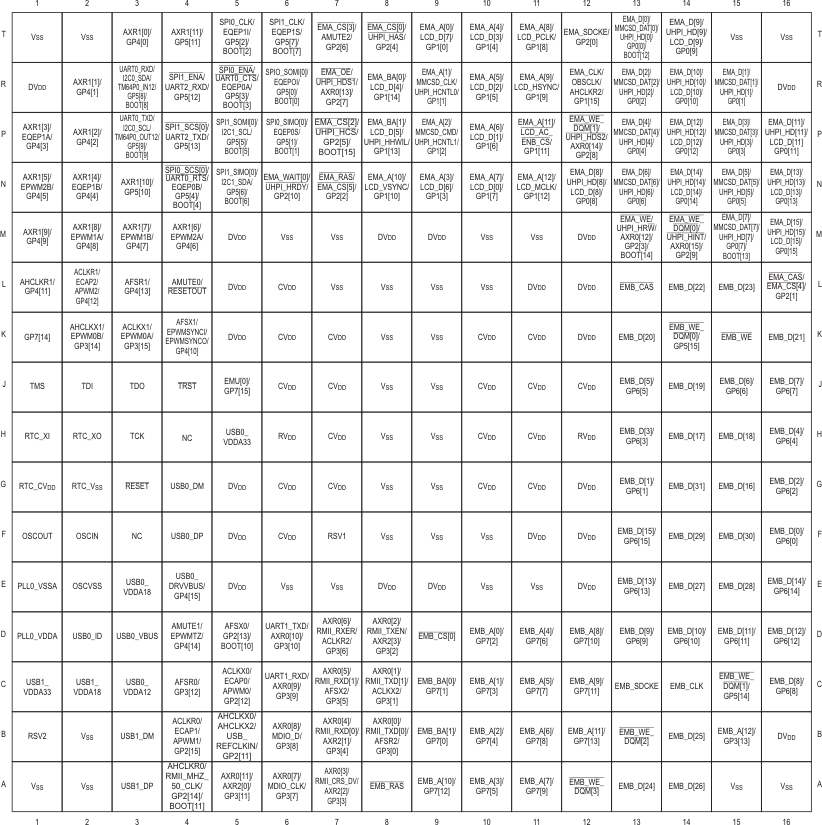 Figure 3-3 Pin Map (ZKB)
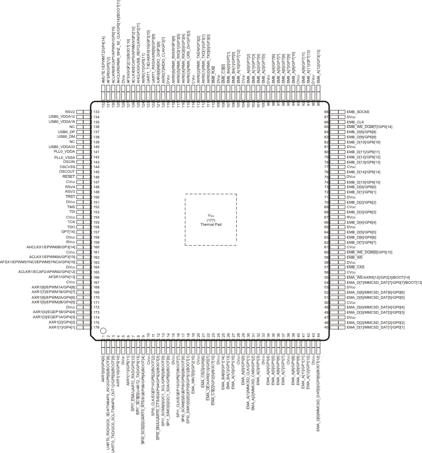 Figure 3-4 Pin Map (PTP)
3.6 Terminal Functions
to identify the external signal names, the associated pin/ball numbers along with the mechanical package designator, the pin type (I, O, IO, OZ, or PWR), whether the pin/ball has any internal pullup/pulldown resistors, whether the pin/ball is configurable as an IO in GPIO mode, and a functional pin description.
3.6.1 Device Reset and JTAG
Table 3-6 Reset and JTAG Terminal Functions
| SIGNAL NAME | PIN NO | TYPE(1) | PULL(2) | DESCRIPTION | |
|---|---|---|---|---|---|
| PTP | ZKB | ||||
| RESET | |||||
| RESET | 146 | G3 | I | Device reset input | |
| AMUTE0/RESETOUT | - | L4 | O(3) | IPD | Reset output |
| JTAG | |||||
| TMS | 152 | J1 | I | IPU | JTAG test mode select |
| TDI | 153 | J2 | I | IPU | JTAG test data input |
| TDO | 156 | J3 | O | IPD | JTAG test data output |
| TCK | 155 | H3 | I | IPU | JTAG test clock |
| TRST | 150 | J4 | I | IPD | JTAG test reset |
| EMU[0]/GP7[15] | - | J5 | I/O | IPU | Emulation Signal |
Note: For multiplexed pins where functions have different types (ie., input versus output), the table reflects the pin function direction for that particular peripheral.
3.6.2 High-Frequency Oscillator and PLL
Table 3-7 High-Frequency Oscillator and PLL Terminal Functions
| SIGNAL NAME | PIN NO | TYPE(1) | PULL(2) | DESCRIPTION | |
|---|---|---|---|---|---|
| PTP | ZKB | ||||
| EMA_CLK/OBSCLK/AHCLKR2/GP1[15] | - | R12 | O | IPU | PLL Observation Clock |
| 1.2-V OSCILLATOR | |||||
| OSCIN | 143 | F2 | I | Oscillator input | |
| OSCOUT | 145 | F1 | O | Oscillator output | |
| OSCVSS | 144 | E2 | GND | Oscillator ground (for filter only) | |
| 1.2-V PLL | |||||
| PLL0_VDDA | 141 | D1 | PWR | PLL analog VDD (1.2-V filtered supply) | |
| PLL0_VSSA | 142 | E1 | GND | PLL analog VSS (for filter) | |
Note: For multiplexed pins where functions have different types (ie., input versus output), the table reflects the pin function direction for that particular peripheral.
3.6.3 Real-Time Clock and 32-kHz Oscillator
Table 3-8 Real-Time Clock (RTC) and 1.2-V, 32-kHz Oscillator Terminal Functions
| SIGNAL NAME | PIN NO | TYPE(1) | PULL(2) | DESCRIPTION | |
|---|---|---|---|---|---|
| PTP | ZKB | ||||
| RTC_CVDD | - | G1 | PWR | RTC module core power (isolated from rest of chip CVDD) | |
| RTC_XI | - | H1 | I | Low-frequency (32-kHz) oscillator receiver for real-time clock | |
| RTC_XO | - | H2 | O | Low-frequency (32-kHz) oscillator driver for real-time clock | |
| RTC_Vss | - | G2 | GND | Oscillator ground (for filter) | |
Note: For multiplexed pins where functions have different types (ie., input versus output), the table reflects the pin function direction for that particular peripheral.
3.6.4 External Memory Interface A (ASYNC, SDRAM)
Table 3-9 External Memory Interface A (EMIFA) Terminal Functions
| SIGNAL NAME | PIN NO | TYPE(1) | PULL(2) | MUXED | DESCRIPTION | |
|---|---|---|---|---|---|---|
| PTP | ZKB | |||||
| EMA_D[15]/UHPI_HD[15]/LCD_D[15]/GP0[15] | - | M16 | I/O | IPD | UHPI, LCD, GPIO | EMIFA data bus |
| EMA_D[14]/UHPI_HD[14]/LCD_D[14]/GP0[14] | - | N14 | I/O | IPD | ||
| EMA_D[13]/UHPI_HD[13]/LCD_D[13]/GP0[13] | - | N16 | I/O | IPD | ||
| EMA_D[12]/UHPI_HD[12]/LCD_D[12]/GP0[12] | - | P14 | I/O | IPD | ||
| EMA_D[11]/UHPI_HD[11]/LCD_D[11]/GP0[11] | - | P16 | I/O | IPD | ||
| EMA_D[10]/UHPI_HD[10]/LCD_D[10]/GP0[10] | - | R14 | I/O | IPD | ||
| EMA_D[9]/UHPI_HD[9]/LCD_D[9]/GP0[9] | - | T14 | I/O | IPD | ||
| EMA_D[8]/UHPI_HD[8]/LCD_D[8]/GP0[8] | - | N12 | I/O | IPD | ||
| EMA_D[7]/MMCSD_DAT[7]/UHPI_HD[7]/GP0[7]/BOOT[13] | 54 | M15 | I/O | IPU | MMC/SD, UHPI, GPIO, BOOT | |
| EMA_D[6]/MMCSD_DAT[6]/UHPI_HD[6]/GP0[6] | 52 | N13 | I/O | IPU | MMC/SD, UHPI, GPIO | |
| EMA_D[5]/MMCSD_DAT[5]/UHPI_HD[5]/GP0[5] | 51 | N15 | I/O | IPU | ||
| EMA_D[4]/MMCSD_DAT[4]/UHPI_HD[4]/GP0[4] | 49 | P13 | I/O | IPU | ||
| EMA_D[3]/MMCSD_DAT[3]/UHPI_HD[3]/GP0[3] | 48 | P15 | I/O | IPU | ||
| EMA_D[2]/MMCSD_DAT[2]/UHPI_HD[2]/GP0[2] | 46 | R13 | I/O | IPU | ||
| EMA_D[1]/MMCSD_DAT[1]/UHPI_HD[1]/GP0[1] | 45 | R15 | I/O | IPU | ||
| EMA_D[0]/MMCSD_DAT[0]/UHPI_HD[0]/GP0[0]/BOOT[12] | 44 | T13 | I/O | IPU | MMC/SD, UHPI, GPIO, BOOT | |
| EMA_A[12]/LCD_MCLK/GP1[12] | 42 | N11 | O | IPU | LCD, GPIO | EMIFA address bus |
| EMA_A[11] /LCD_AC_ENB_CS/GP1[11] | 41 | P11 | O | IPU | ||
| EMA_A[10]/LCD_VSYNC/GP1[10] | 27 | N8 | O | IPU | ||
| EMA_A[9]/LCD_HSYNC/GP1[9] | 40 | R11 | O | IPU | ||
| EMA_A[8]/LCD_PCLK/GP1[8] | 39 | T11 | O | IPU | ||
| EMA_A[7]/LCD_D[0]/GP1[7] | 37 | N10 | O | IPD | ||
| EMA_A[6]/LCD_D[1]/GP1[6] | 36 | P10 | O | IPD | ||
| EMA_A[5]/LCD_D[2]/GP1[5] | 35 | R10 | O | IPD | ||
| EMA_A[4]/LCD_D[3]/GP1[4] | 34 | T10 | O | IPD | ||
| EMA_A[3]/LCD_D[6]/GP1[3] | 32 | N9 | O | IPD | ||
| EMA_A[2]/MMCSD_CMD/UHPI_HCNTL1/GP1[2] | 31 | P9 | O | IPU | MMCSD, UHPI, GPIO | EMIFA address bus |
| EMA_A[1]/MMCSD_CLK/UHPI_HCNTL0/GP1[1] | 30 | R9 | O | IPU | ||
| EMA_A[0]/LCD_D[7]/GP1[0] | 29 | T9 | O | IPD | LCD, GPIO | |
| EMA_BA[1]/LCD_D[5]/UHPI_HHWIL/GP1[13] | 26 | P8 | O | IPU | LCD, UHPI, GPIO | EMIFA bank address |
| EMA_BA[0]/LCD_D[4]/GP1[14] | 25 | R8 | O | IPU | LCD, GPIO | |
| EMA_CLK/OBSCLK/AHCLKR2/GP1[15] | - | R12 | O | IPU | McASP2, GPIO | EMIFA clock |
| EMA_SDCKE/GP2[0] | - | T12 | O | IPU | GPIO | EMIFA SDRAM clock enable |
| EMA_RAS/EMA_CS[5]/GP2[2] | - | N7 | O | IPU | EMIF A chip select, GPIO | EMIFA SDRAM row address strobe |
| EMA_CAS/EMA_CS[4]/GP2[1] | - | L16 | O | IPU | EMIFA SDRAM column address strobe | |
| EMA_RAS/EMA_CS[5]/GP2[2] | - | N7 | O | IPU | EMIF A SDRAM, GPIO | EMIFA Async Chip Select |
| EMA_CAS/EMA_CS[4]/GP2[1] | - | L16 | O | IPU | ||
| EMA_CS[3]/AMUTE2/GP2[6] | 21 | T7 | O | IPU | McASP2, GPIO | |
| EMA_CS[2]/UHPI_HCS/GP2[5]/BOOT[15] | 23 | P7 | O | IPU | UHPI, GPIO, BOOT | |
| EMA_CS[0]/UHPI_HAS/GP2[4] | - | T8 | O | IPU | UHPI, GPIO | EMIFA SDRAM chip select |
| EMA_WE/UHPI_HRW/AXR0[12]/GP2[3]/BOOT[14] | 55 | M13 | O | IPU | UHPI, MCASP0, GOPIO, BOOT | EMIFA SDRAM write enable |
| EMA_WE_DQM[1]/UHPI_HDS2/AXR0[14]/GP2[8] | - | P12 | O | IPU | UHPI, McASP, GPIO | EMIFA write enable/data mask for EMA_D[15:8] |
| EMA_WE_DQM[0]/UHPI_HINT/AXR0[15]/GP2[9] | - | M14 | O | IPU | EMIFA write enable/data mask for EMA_D[7:0] | |
| EMA_OE/UHPI_HDS1/AXR0[13]/GP2[7] | 22 | R7 | O | IPU | UHPI, McASP0, GPIO | EMIFA output enable |
| EMA_WAIT[0]/ UHPI_HRDY/GP2[10] | 19 | N6 | I | IPU | UHPI, GPIO | EMIFA wait input/interrupt |
Note: The pin type shown refers to the input, output or high-impedance state of the pin function when configured as the the signal name highlighted in bold. All multiplexed signals may enter a high-impedance state when the configured function is input-only or the configured function supports high-Z operation. All GPIO signals can be used as input or output. For multiplexed pins where functions have different types (ie., input versus output), the table reflects the pin function direction for that particular peripheral.
3.6.5 External Memory Interface B (only SDRAM)
Table 3-10 External Memory Interface B (EMIFB) Terminal Functions
| SIGNAL NAME | PIN NO | TYPE(1) | PULL(2) | MUXED | DESCRIPTION | |
|---|---|---|---|---|---|---|
| PTP | ZKB | |||||
| EMB_D[31] | - | G14 | I/O | IPD | EMIFB SDRAM data bus | |
| EMB_D[30] | - | F15 | I/O | IPD | ||
| EMB_D[29] | - | F14 | I/O | IPD | ||
| EMB_D[28] | - | E15 | I/O | IPD | ||
| EMB_D[27] | - | E14 | I/O | IPD | ||
| EMB_D[26] | - | A14 | I/O | IPD | ||
| EMB_D[25] | - | B14 | I/O | IPD | ||
| EMB_D[24] | - | A13 | I/O | IPD | ||
| EMB_D[23] | - | L15 | I/O | IPD | ||
| EMB_D[22] | - | L14 | I/O | IPD | ||
| EMB_D[21] | - | K16 | I/O | IPD | ||
| EMB_D[20] | - | K13 | I/O | IPD | ||
| EMB_D[19] | - | J14 | I/O | IPD | ||
| EMB_D[18] | - | H15 | I/O | IPD | ||
| EMB_D[17] | - | H14 | I/O | IPD | ||
| EMB_D[16] | - | G15 | I/O | IPD | ||
| EMB_D[15]/GP6[15] | 74 | F13 | I/O | IPD | GPIO | |
| EMB_D[14]/GP6[14] | 76 | E16 | I/O | IPD | ||
| EMB_D[13]/GP6[13] | 78 | E13 | I/O | IPD | ||
| EMB_D[12]/GP6[12] | 79 | D16 | I/O | IPD | ||
| EMB_D[11]/GP6[11] | 80 | D15 | I/O | IPD | ||
| EMB_D[10]/GP6[10] | 82 | D14 | I/O | IPD | ||
| EMB_D[9]/GP6[9] | 83 | D13 | I/O | IPD | ||
| EMB_D[8]/GP6[8] | 84 | C16 | I/O | IPD | ||
| EMB_D[7]/GP6[7] | 62 | J16 | I/O | IPD | ||
| EMB_D[6]/GP6[6] | 63 | J15 | I/O | IPD | ||
| EMB_D[5]/GP6[5] | 64 | J13 | I/O | IPD | ||
| EMB_D[4]/GP6[4] | 66 | H16 | I/O | IPD | ||
| EMB_D[3]/GP6[3] | 68 | H13 | I/O | IPD | ||
| EMB_D[2]/GP6[2] | 70 | G16 | I/O | IPD | ||
| EMB_D[1]/GP6[1] | 72 | G13 | I/O | IPD | ||
| EMB_D[0]/GP6[0] | 73 | F16 | I/O | IPD | ||
| EMB_A[12]/GP3[13] | 89 | B15 | O | IPD | GPIO | EMIFB SDRAM row/column address bus |
| EMB_A[11]/GP7[13] | 91 | B12 | O | IPD | ||
| EMB_A[10]/GP7[12] | 105 | A9 | O | IPD | ||
| EMB_A[9]/GP7[11] | 92 | C12 | O | IPD | ||
| EMB_A[8]/GP7[10] | 94 | D12 | O | IPD | ||
| EMB_A[7]/GP7[9] | 95 | A11 | O | IPD | ||
| EMB_A[6]/GP7[8] | 96 | B11 | O | IPD | ||
| EMB_A[5]/GP7[7] | 97 | C11 | O | IPD | ||
| EMB_A[4]/GP7[6] | 98 | D11 | O | IPD | GPIO | EMIFB SDRAM row/column address |
| EMB_A[3]/GP7[5] | 100 | A10 | O | IPD | ||
| EMB_A[2]/GP7[4] | 101 | B10 | O | IPD | ||
| EMB_A[1]/GP7[3] | 102 | C10 | O | IPD | ||
| EMB_A[0]/GP7[2] | 103 | D10 | O | IPD | ||
| EMB_BA[1]/GP7[0] | 106 | B9 | O | IPU | EMIFB SDRAM bank address | |
| EMB_BA[0]/GP7[1] | 107 | C9 | O | IPU | ||
| EMB_CLK | 86 | C14 | O | IPU | EMIF SDRAM clock | |
| EMB_SDCKE | 88 | C13 | O | IPU | EMIFB SDRAM clock enable | |
| EMB_WE | 59 | K15 | O | IPU | EMIFB write enable | |
| EMB_RAS | 110 | A8 | O | IPU | EMIFB SDRAM row address strobe | |
| EMB_CAS | 57 | L13 | O | IPU | EMIFB column address strobe | |
| EMB_CS[0] | 108 | D9 | O | IPU | EMIFB SDRAM chip select 0 | |
| EMB_WE_DQM[3] | - | A12 | O | IPU | EMIFB write enable/data mask for EMB_D | |
| EMB_WE_DQM[2] | - | B13 | O | IPU | ||
| EMB_WE_DQM[1]/GP5[14] | 85 | C15 | O | IPU | GPIO | |
| EMB_WE_DQM[0]/GP5[15] | 60 | K14 | O | IPU | ||
Note: The pin type shown refers to the input, output or high-impedance state of the pin function when configured as the the signal name highlighted in bold. All multiplexed signals may enter a high-impedance state when the configured function is input-only or the configured function supports high-Z operation. All GPIO signals can be used as input or output. For multiplexed pins where functions have different types (ie., input versus output), the table reflects the pin function direction for that particular peripheral.
3.6.6 Serial Peripheral Interface Modules (SPI0, SPI1)
Table 3-11 Serial Peripheral Interface (SPI) Terminal Functions
| SIGNAL NAME | PIN NO | TYPE(1) | PULL(2) | MUXED | DESCRIPTION | |
|---|---|---|---|---|---|---|
| PTP | ZKB | |||||
| SPI0 | ||||||
| SPI0_SCS[0]/UART0_RTS/EQEP0B/GP5[4]/BOOT[4] | 9 | N4 | I/O | IPU | UART0, EQEP0B, GPIO, BOOT | SPI0 chip select |
| SPI0_ENA/UART0_CTS/EQEP0A/GP5[3]/BOOT[3] | 12 | R5 | I/O | IPU | UART0, EQEP0A, GPIO, BOOT | SPI0 enable |
| SPI0_CLK/EQEP1I/GP5[2]/BOOT[2] | 11 | T5 | I/O | IPD | eQEP1, GPIO, BOOT | SPI0 clock |
| SPI0_SIMO[0]/EQEP0S/GP5[1]/BOOT[1] | 18 | P6 | I/O | IPD | eQEP0, GPIO, BOOT | SPI0 data slave-in-master-out |
| SPI0_SOMI[0]/EQEP0I/GP5[0]/BOOT[0] | 17 | R6 | I/O | IPD | SPI0 data slave-out-master-in | |
| SPI1 | ||||||
| SPI1_SCS[0]/UART2_TXD/GP5[13] | 8 | P4 | I/O | IPU | UART2, GPIO | SPI1 chip select |
| SPI1_ENA/UART2_RXD/GP5[12] | 7 | R4 | I/O | IPU | SPI1 enable | |
| SPI1_CLK/EQEP1S/GP5[7]/BOOT[7] | 16 | T6 | I/O | IPD | eQEP1, GPIO, BOOT | SPI1 clock |
| SPI1_SIMO[0]/I2C1_SDA/GP5[6]/BOOT[6] | 14 | N5 | I/O | IPU | I2C1, GPIO, BOOT | SPI1 data slave-in-master-out |
| SPI1_SOMI[0]/I2C1_SCL/GP5[5]/BOOT[5] | 13 | P5 | I/O | IPU | SPI1 data slave-out-master-in | |
Note: The pin type shown refers to the input, output or high-impedance state of the pin function when configured as the the signal name highlighted in bold. All multiplexed signals may enter a high-impedance state when the configured function is input-only or the configured function supports high-Z operation. All GPIO signals can be used as input or output. For multiplexed pins where functions have different types (ie., input versus output), the table reflects the pin function direction for that particular peripheral.
3.6.7 Enhanced Capture/Auxiliary PWM Modules (eCAP0, eCAP1, eCAP2)
The eCAP Module pins function as either input captures or auxiliary PWM 32-bit outputs, depending upon how the eCAP module is programmed.
Table 3-12 Enhanced Capture Module (eCAP) Terminal Functions
| SIGNAL NAME | PIN NO | TYPE(1) | PULL(2) | MUXED | DESCRIPTION | |
|---|---|---|---|---|---|---|
| PTP | ZKB | |||||
| eCAP0 | ||||||
| ACLKX0/ECAP0/APWM0/GP2[12] | 126 | C5 | I/O | IPD | McASP0, GPIO | enhanced capture 0 input or auxiliary PWM 0 output |
| eCAP1 | ||||||
| ACLKR0/ECAP1/APWM1/GP2[15] | 130 | B4 | I/O | IPD | McASP0, GPIO | enhanced capture 1 input or auxiliary PWM 1 output |
| eCAP2 | ||||||
| ACLKR1/ECAP2/APWM2/GP4[12] | 165 | L2 | I/O | IPD | McASP1, GPIO | enhanced capture 2 input or auxiliary PWM 2 output |
Note: The pin type shown refers to the input, output or high-impedance state of the pin function when configured as the the signal name highlighted in bold. All multiplexed signals may enter a high-impedance state when the configured function is input-only or the configured function supports high-Z operation. All GPIO signals can be used as input or output. For multiplexed pins where functions have different types (ie., input versus output), the table reflects the pin function direction for that particular peripheral.
3.6.8 Enhanced Pulse Width Modulators (eHRPWM0, eHRPWM1, eHRPWM2)
Table 3-13 Enhanced Pulse Width Modulator (eHRPWM) Terminal Functions
| SIGNAL NAME | PIN NO | TYPE(1) | PULL(2) | MUXED | DESCRIPTION | |
|---|---|---|---|---|---|---|
| PTP | ZKB | |||||
| eHRPWM0 | ||||||
| ACLKX1/EPWM0A/GP3[15] | 162 | K3 | I/O | IPD | McASP1, GPIO | eHRPWM0 A output (with high-resolution) |
| AHCLKX1/EPWM0B/GP3[14] | 160 | K2 | I/O | IPD | eHRPWM0 B output. | |
| AMUTE1/EPWMTZ/GP4[14] | 132 | D4 | I/O | IPD | McASP1, eHRPWM1, GPIO, eHRPWM2 | eHRPWM0 trip zone input |
| AFSX1/EPWMSYNCI/EPWMSYNCO/GP4[10] | 163 | K4 | I/O | IPD | McASP1, eHRPWM0, GPIO | Sync input to eHRPWM0 module or sync output to external PWM |
| eHRPWM1 | ||||||
| AXR1[8]/EPWM1A/GP4[8] | 168 | M2 | I/O | IPD | McASP1, GPIO | eHRPWM1 A (with high-resolution) |
| AXR1[7]/EPWM1B/GP4[7] | 169 | M3 | I/O | IPD | eHRPWM1 B output | |
| AMUTE1/EPWMTZ/GP4[14] | 132 | D4 | I/O | IPD | McASP1, eHRPWM0, GPIO, eHRPWM2 | eHRPWM1 trip zone input |
| eHRPWM2 | ||||||
| AXR1[6]/EPWM2A/GP4[6] | 170 | M4 | I/O | IPD | McASP1, GPIO | eHRPWM2 A (with high-resolution) |
| AXR1[5]/EPWM2B/GP4[5] | 171 | N1 | I/O | IPD | eHRPWM2 B output | |
| AMUTE1/EPWMTZ/GP4[14] | 132 | D4 | I/O | IPD | McASP1, eHRPWM0, GPIO, eHRPWM2 | eHRPWM2 trip zone input |
Note: The pin type shown refers to the input, output or high-impedance state of the pin function when configured as the the signal name highlighted in bold. All multiplexed signals may enter a high-impedance state when the configured function is input-only or the configured function supports high-Z operation. All GPIO signals can be used as input or output. For multiplexed pins where functions have different types (ie., input versus output), the table reflects the pin function direction for that particular peripheral.
3.6.9 Enhanced Quadrature Encoder Pulse Module (eQEP)
Table 3-14 Enhanced Quadrature Encoder Pulse Module (eQEP) Terminal Functions
| SIGNAL NAME | PIN NO | TYPE(1) | PULL(2) | MUXED | DESCRIPTION | |
|---|---|---|---|---|---|---|
| PTP | ZKB | |||||
| eQEP0 | ||||||
| SPI0_ENA/UART0_CTS/EQEP0A/GP5[3]/BOOT[3] | 12 | R5 | I | IPU | SPI0, UART0, GPIO, BOOT | eQEP0A quadrature input |
| SPI0_SCS[0]/UART0_RTS/EQEP0B/GP5[4]/BOOT[4] | 9 | N4 | I | IPU | eQEP0B quadrature input | |
| SPI0_SOMI[0]/EQEP0I/GP5[0]/BOOT[0] | 17 | R6 | I | IPD | SPI0, GPIO, BOOT | eQEP0 index |
| SPI0_SIMO[0]/EQEP0S/GP5[1]/BOOT[1] | 18 | P6 | I | IPD | eQEP0 strobe | |
| eQEP1 | ||||||
| AXR1[3]/EQEP1A/GP4[3] | 174 | P1 | I | IPD | McASP1, GPIO | eQEP1A quadrature input |
| AXR1[4]/EQEP1B/GP4[4] | 173 | N2 | I | IPD | eQEP1B quadrature input | |
| SPI0_CLK/EQEP1I/GP5[2]/BOOT[2] | 11 | T5 | I | IPD | SPI0, GPIO, BOOT | eQEP1 index |
| SPI1_CLK/EQEP1S/GP5[7]/BOOT[7] | 16 | T6 | I | IPD | SPI1, GPIO, BOOT | eQEP1 strobe |
Note: The pin type shown refers to the input, output or high-impedance state of the pin function when configured as the the signal name highlighted in bold. All multiplexed signals may enter a high-impedance state when the configured function is input-only or the configured function supports high-Z operation. All GPIO signals can be used as input or output. For multiplexed pins where functions have different types (ie., input versus output), the table reflects the pin function direction for that particular peripheral.
3.6.10 Boot
Table 3-15 Boot Terminal Functions(3)
| SIGNAL NAME | PIN NO | TYPE(1) | PULL(2) | MUXED | DESCRIPTION | |
|---|---|---|---|---|---|---|
| PTP | ZKB | |||||
| EMA_CS[2]/UHPI_HCS/GP2[5]/BOOT[15] | 23 | P7 | I | IPU | EMIFA, UHPI, GPIO | BOOT[15] |
| EMA_WE/UHPI_HRW/AXR0[12]/GP2[3]/BOOT[14] | 55 | M13 | I | IPU | EMIFA, UHPI, McASP0, GPIO | BOOT[14] |
| EMA_D[7]/MMCSD_DAT[7]/UHPI_HD[7]/GP0[7]/BOOT[13] | 54 | M15 | I | IPU | EMIFA, MMC/SD, UHPI, GPIO | BOOT[13] |
| EMA_D[0]/MMCSD_DAT[0]/UHPI_HD[0]/GP0[0]/BOOT[12] | 44 | T13 | I | IPU | BOOT[12] | |
| AHCLKR0/RMII_MHZ_50_CLK/GP2[14]/BOOT[11] | 129 | A4 | I | IPD | McASP0, EMAC, GPIO | BOOT[11] |
| AFSX0/GP2[13]/BOOT[10] | 127 | D5 | I | IPD | McASP0, GPIO | BOOT[10] |
| UART0_TXD/I2C0_SCL/TM64P0_OUT12/GP5[9]/BOOT[9] | 3 | P3 | I | IPU | UART0, I2C0, Timer0, GPIO | BOOT[9] |
| UART0_RXD/I2C0_SDA/TM64P0_IN12/GP5[8]/BOOT[8] | 2 | R3 | I | IPU | UART0, I2C0, Timer0, GPIO | BOOT[8] |
| SPI1_CLK/EQEP1S/GP5[7]/BOOT[7] | 16 | T6 | I | IPD | SPI1, eQEP1, GPIO | BOOT[7] |
| SPI1_SIMO[0]/I2C1_SDA/GP5[6]/BOOT[6] | 14 | N5 | I | IPU | SPI1, I2C1, GPIO | BOOT[6] |
| SPI1_SOMI[0]/I2C1_SCL/GP5[5]/BOOT[5] | 13 | P5 | I | IPU | BOOT[5] | |
| SPI0_SCS[0]/UART0_RTS/EQEP0B/GP5[4]/BOOT[4] | 9 | N4 | I | IPU | SPI0, UART0, eQEP0, GPIO | BOOT[4] |
| SPI0_ENA/UART0_CTS/EQEP0A/GP5[3]/BOOT[3] | 12 | R5 | I | IPU | SPI0, UART0, eQEP0, GPIO | BOOT[3] |
| SPI0_CLK/EQEP1I/GP5[2]/BOOT[2] | 11 | T5 | I | IPD | SPI0, eQEP1, GPIO | BOOT[2] |
| SPI0_SIMO[0]/EQEP0S/GP5[1]/BOOT[1] | 18 | P6 | I | IPD | SPI0, eQEP0, GPIO | BOOT[1] |
| SPI0_SOMI[0]/EQEP0I/GP5[0]/BOOT[0] | 17 | R6 | I | IPD | BOOT[0] | |
Note: The pin type shown refers to the input, output or high-impedance state of the pin function when configured as the the signal name highlighted in bold. All multiplexed signals may enter a high-impedance state when the configured function is input-only or the configured function supports high-Z operation. All GPIO signals can be used as input or output. For multiplexed pins where functions have different types (ie., input versus output), the table reflects the pin function direction for that particular peripheral.
3.6.11 Universal Asynchronous Receiver/Transmitters (UART0, UART1, UART2)
Table 3-16 Universal Asynchronous Receiver/Transmitter (UART) Terminal Functions
| SIGNAL NAME | PIN NO | TYPE(1) | PULL(2) | MUXED | DESCRIPTION | |
|---|---|---|---|---|---|---|
| PTP | ZKB | |||||
| UART0 | ||||||
| UART0_RXD/I2C0_SDA/TM64P0_IN12/GP5[8]/BOOT[8] | 2 | R3 | I | IPU | I2C0, BOOT, Timer0, GPIO, | UART0 receive data |
| UART0_TXD/I2C0_SCL/TM64P0_OUT12/GP5[9]/BOOT[9] | 3 | P3 | O | IPU | I2C0, Timer0, GPIO, BOOT | UART0 transmit data |
| SPI0_SCS[0]/UART0_RTS/EQEP0B/GP5[4]/BOOT[4] | 9 | N4 | O | IPU | SPI0, eQEP0, GPIO, BOOT | UART0 ready-to-send output |
| SPI0_ENA/UART0_CTS/EQEP0A/GP5[3]/BOOT[3] | 12 | R5 | I | IPU | UART0 clear-to-send input | |
| UART1 | ||||||
| UART1_RXD/AXR0[9]/GP3[9](3) | 122 | C6 | I | IPD | McASP0, GPIO | UART1 receive data |
| UART1_TXD/AXR0[10]/GP3[10](3) | 123 | D6 | O | IPD | UART1 transmit data | |
| UART2 | ||||||
| SPI1_ENA/UART2_RXD/GP5[12] | 7 | R4 | I | IPU | SPI1, GPIO | UART2 receive data |
| SPI1_SCS[0]/UART2_TXD/GP5[13] | 8 | P4 | O | IPU | UART2 transmit data | |
Note: The pin type shown refers to the input, output or high-impedance state of the pin function when configured as the the signal name highlighted in bold. All multiplexed signals may enter a high-impedance state when the configured function is input-only or the configured function supports high-Z operation. All GPIO signals can be used as input or output. For multiplexed pins where functions have different types (ie., input versus output), the table reflects the pin function direction for that particular peripheral.
3.6.12 Inter-Integrated Circuit Modules (I2C0, I2C1)
Table 3-17 Inter-Integrated Circuit (I2C) Terminal Functions
| SIGNAL NAME | PIN NO | TYPE(1) | PULL(2) | MUXED | DESCRIPTION | |
|---|---|---|---|---|---|---|
| PTP | ZKB | |||||
| I2C0 | ||||||
| UART0_RXD/I2C0_SDA/TM64P0_IN12/GP5[8]/BOOT[8] | 2 | R3 | I/O | IPU | UART0, Timer0, GPIO, BOOT | I2C0 serial data |
| UART0_TXD/I2C0_SCL/TM64P0_OUT12/GP5[9]/BOOT[9] | 3 | P3 | I/O | IPU | UART0, Timer0, GPIO, BOOT | I2C0 serial clock |
| I2C1 | ||||||
| SPI1_SIMO[0]/I2C1_SDA/GP5[6]/BOOT[6] | 14 | N5 | I/O | IPU | SPI1, GPIO, BOOT | I2C1 serial data |
| SPI1_SOMI[0]/I2C1_SCL/GP5[5]/BOOT[5] | 13 | P5 | I/O | IPU | I2C1 serial clock | |
Note: The pin type shown refers to the input, output or high-impedance state of the pin function when configured as the the signal name highlighted in bold. All multiplexed signals may enter a high-impedance state when the configured function is input-only or the configured function supports high-Z operation. All GPIO signals can be used as input or output. For multiplexed pins where functions have different types (ie., input versus output), the table reflects the pin function direction for that particular peripheral.
3.6.13 Timers
Table 3-18 Timers Terminal Functions
| SIGNAL NAME | PIN NO | TYPE(1) | PULL(2) | MUXED | DESCRIPTION | |
|---|---|---|---|---|---|---|
| PTP | ZKB | |||||
| TIMER0 | ||||||
| UART0_RXD/I2C0_SDA/TM64P0_IN12/GP5[8]/BOOT[8] | 2 | R3 | I | IPU | UART0, I2C0, GPIO, BOOT | Timer0 lower input |
| UART0_TXD/I2C0_SCL/TM64P0_OUT12/GP5[9]/BOOT[9] | 3 | P3 | O | IPU | Timer0 lower output | |
| TIMER1 (Watchdog ) | ||||||
| No external pins. The Timer1 peripheral pins are not pinned out as external pins. | ||||||
Note: The pin type shown refers to the input, output or high-impedance state of the pin function when configured as the the signal name highlighted in bold. All multiplexed signals may enter a high-impedance state when the configured function is input-only or the configured function supports high-Z operation. All GPIO signals can be used as input or output. For multiplexed pins where functions have different types (ie., input versus output), the table reflects the pin function direction for that particular peripheral.
3.6.14 Universal Host-Port Interface (UHPI)
Note:
The UHPI module requires 16 data pins for the host port interface to function. Therefore on the PTP, the UHPI is not available.
Table 3-19 Universal Host-Port Interface (UHPI) Terminal Functions
| SIGNAL NAME | PIN NO | TYPE(1) | PULL(2) | MUXED | DESCRIPTION | |
|---|---|---|---|---|---|---|
| PTP | ZKB | |||||
| EMA_D[15]/UHPI_HD[15]/LCD_D[15]/GP0[15] | - | M16 | I/O | IPD | EMIFA, LCD, GPIO | UHPI data bus |
| EMA_D[14]/UHPI_HD[14]/LCD_D[14]/GP0[14] | - | N14 | I/O | IPD | ||
| EMA_D[13]/UHPI_HD[13]/LCD_D[13]/GP0[13] | - | N16 | I/O | IPD | ||
| EMA_D[12]/UHPI_HD[12]/LCD_D[12]/GP0[12] | - | P14 | I/O | IPD | ||
| EMA_D[11]/UHPI_HD[11]/LCD_D[11]/GP0[11] | - | P16 | I/O | IPD | ||
| EMA_D[10]/UHPI_HD[10]/LCD_D[10]/GP0[10] | - | R14 | I/O | IPD | ||
| EMA_D[9]/UHPI_HD[9]/LCD_D[9]/GP0[9] | - | T14 | I/O | IPD | ||
| EMA_D[8]/UHPI_HD[8]/LCD_D[8]/GP0[8] | - | N12 | I/O | IPD | ||
| EMA_D[7]/MMCSD_DAT[7]/UHPI_HD[7]/GP0[7]/ BOOT[13] |
- | M15 | I/O | IPU | EMIFA, MMC/SD, GPIO, BOOT | |
| EMA_D[6]/MMCSD_DAT[6]/UHPI_HD[6]/GP0[6] | - | N13 | I/O | IPU | EMIFA, MMC/SD, GPIO | |
| EMA_D[5]/MMCSD_DAT[5]/UHPI_HD[5]/GP0[5] | - | N15 | I/O | IPU | ||
| EMA_D[4]/MMCSD_DAT[4]/UHPI_HD[4]/GP0[4] | - | P13 | I/O | IPU | ||
| EMA_D[3]/MMCSD_DAT[3]/UHPI_HD[3]/GP0[3] | - | P15 | I/O | IPU | ||
| EMA_D[2]/MMCSD_DAT[2]/UHPI_HD[2]/GP0[2] | - | R13 | I/O | IPU | ||
| EMA_D[1]/MMCSD_DAT[1]/UHPI_HD[1]/GP0[1] | - | R15 | I/O | IPU | ||
| EMA_D[0]/MMCSD_DAT[0]/UHPI_HD[0]/GP0[0]/ BOOT[12] |
- | T13 | I/O | IPU | EMIFA, MMC/SD, GPIO, BOOT | |
| EMA_A[2]/MMCSD_CMD/UHPI_HCNTL1/GP1[2] | - | P9 | I/O | IPU | EMIFA, MMCSD_CMD, GPIO | UHPI access control |
| EMA_A[1]/MMCSD_CLK/UHPI_HCNTL0/GP1[1] | - | R9 | I/O | IPU | ||
| EMA_BA[1]/LCD_D[5]/UHPI_HHWIL/GP1[13] | - | P8 | I/O | IPU | EMIFA, LCD, GPIO | UHPI half-word identification control |
| EMA_WE/UHPI_HRW/AXR0[12]/GP2[3]/BOOT[14] | - | M13 | I/O | IPU | EMIFA, McASP, GPIO, BOOT | UHPI read/write |
| EMA_CS[2]/UHPI_HCS/GP2[5]/BOOT[15] | - | P7 | I/O | IPU | EMIFA, GPIO, BOOT | UHPI chip select |
| EMA_WE_DQM[1]/UHPI_HDS2/AXR0[14]/GP2[8] | - | P12 | I/O | IPU | EMIFA, McASP0, GPIO | UHPI data strobe |
| EMA_OE/UHPI_HDS1/AXR0[13]/GP2[7] | - | R7 | I/O | IPU | ||
| EMA_WE_DQM[0]/UHPI_HINT/AXR0[15]/GP2[9] | - | M14 | I/O | IPU | UHPI host interrupt | |
| EMA_WAIT[0]/UHPI_HRDY/GP2[10] | - | N6 | I/O | IPU | EMIFA, GPIO | UHPI ready |
| EMA_CS[0]/UHPI_HAS/GP2[4] | - | T8 | I/O | IPU | UHPI address strobe | |
Note: The pin type shown refers to the input, output or high-impedance state of the pin function when configured as the the signal name highlighted in bold. All multiplexed signals may enter a high-impedance state when the configured function is input-only or the configured function supports high-Z operation. All GPIO signals can be used as input or output. For multiplexed pins where functions have different types (ie., input versus output), the table reflects the pin function direction for that particular peripheral.
3.6.15 Multichannel Audio Serial Ports (McASP0, McASP1, McASP2)
Table 3-20 Multichannel Audio Serial Ports (McASPs) Terminal Functions
| SIGNAL NAME | PIN NO | TYPE(1) | PULL(2) | MUXED | DESCRIPTION | ||
|---|---|---|---|---|---|---|---|
| PTP | ZKB | ||||||
| McASP0 | |||||||
| EMA_WE_DQM[0]/UHPI_HINT/AXR0[15]/GP2[9] | - | M14 | I/O | IPU | EMIFA, UHPI, GPIO | McASP0 serial data | |
| EMA_WE_DQM[1]/UHPI_HDS2/AXR0[14]/GP2[8] | - | P12 | I/O | IPU | |||
| EMA_OE/UHPI_HDS1/AXR0[13]/GP2[7] | 22 | R7 | I/O | IPU | |||
| EMA_WE/UHPI_HRW/AXR0[12]/GP2[3]/BOOT[14] | 55 | M13 | I/O | IPU | EMIFA, UHPI, GPIO, BOOT | ||
| AXR0[11]/AXR2[0]/GP3[11] | 124 | A5 | I/O | IPD | McASP2, GPIO | ||
| UART1_TXD/AXR0[10]/GP3[10] | 123 | D6 | I/O | IPD | UART1, GPIO | ||
| UART1_RXD/AXR0[9]/GP3[9] | 122 | C6 | I/O | IPD | UART1, GPIO | ||
| AXR0[8]/MDIO_D/GP3[8] | 121 | B6 | I/O | IPU | MDIO, GPIO | ||
| AXR0[7]/MDIO_CLK/GP3[7] | 120 | A6 | I/O | IPD | |||
| AXR0[6]/RMII_RXER/ACLKR2/GP3[6] | 118 | D7 | I/O | IPD | EMAC, McASP2, GPIO | ||
| AXR0[5]/RMII_RXD[1]/AFSX2/GP3[5] | 117 | C7 | I/O | IPD | |||
| AXR0[4]/RMII_RXD[0]/AXR2[1]/GP3[4] | 116 | B7 | I/O | IPD | |||
| AXR0[3]/RMII_CRS_DV/AXR2[2]/GP3[3] | 115 | A7 | I/O | IPD | |||
| AXR0[2]/RMII_TXEN/AXR2[3]/GP3[2] | 113 | D8 | I/O | IPD | |||
| AXR0[1]/RMII_TXD[1]/ACLKX2/GP3[1] | 112 | C8 | I/O | IPD | |||
| AXR0[0]/RMII_TXD[0]/AFSR2/GP3[0] | 111 | B8 | I/O | IPD | |||
| AHCLKX0/AHCLKX2/USB_REFCLKIN/GP2[11] | 125 | B5 | I/O | IPD | McASP2, USB, GPIO | McASP0 transmit master clock | |
| ACLKX0/ECAP0/APWM0/GP2[12] | 126 | C5 | I/O | IPD | eCAP0, GPIO | McASP0 transmit bit clock | |
| AFSX0/GP2[13]/BOOT[10] | 127 | D5 | I/O | IPD | GPIO, BOOT | McASP0 transmit frame sync | |
| AHCLKR0/RMII_MHZ_50_CLK/GP2[14]/BOOT[11] | 129 | A4 | I/O | IPD | EMAC, GPIO, BOOT | McASP0 receive master clock | |
| ACLKR0/ECAP1/APWM1/GP2[15] | 130 | B4 | I/O | IPD | eCAP1, GPIO | McASP0 receive bit clock | |
| AFSR0/GP3[12] | 131 | C4 | I/O | IPD | GPIO | McASP0 receive frame sync | |
| AMUTE0/RESETOUT | - | L4 | O | IPD | RESETOUT | McASP0 mute output | |
| McASP1 | |||||||
| AXR1[11]/GP5[11] | 6 | T4 | I/O | IPU | GPIO | McASP1 serial data | |
| AXR1[10]/GP5[10] | 4 | N3 | I/O | IPU | |||
| AXR1[9]/GP4[9] | - | M1 | I/O | IPD | |||
| AXR1[8]/EPWM1A/GP4[8] | 168 | M2 | I/O | IPD | eHRPWM1 A, GPIO | ||
| AXR1[7]/EPWM1B/GP4[7] | 169 | M3 | I/O | IPD | eHRPWM1 B, GPIO | ||
| AXR1[6]/EPWM2A/GP4[6] | 170 | M4 | I/O | IPD | eHRPWM2 A, GPIO | ||
| AXR1[5]/EPWM2B/GP4[5] | 171 | N1 | I/O | IPD | eHRPWM2 B, GPIO | ||
| AXR1[4]/EQEP1B/GP4[4] | 173 | N2 | I/O | IPD | eQEP, GPIO | ||
| AXR1[3]/EQEP1A/GP4[3] | 174 | P1 | I/O | IPD | |||
| AXR1[2]/GP4[2] | 175 | P2 | I/O | IPD | GPIO | ||
| AXR1[1]/GP4[1] | 176 | R2 | I/O | IPD | |||
| AXR1[0]/GP4[0] | 1 | T3 | I/O | IPD | |||
| AHCLKX1/EPWM0B/GP3[14] | 160 | K2 | I/O | IPD | eHRPWM0, GPIO | McASP1 transmit master clock | |
| ACLKX1/EPWM0A/GP3[15] | 162 | K3 | I/O | IPD | eHRPWM0, GPIO | McASP1 transmit bit clock | |
| AFSX1/EPWMSYNCI/EPWMSYNCO/GP4[10] | 163 | K4 | I/O | IPD | eHRPWM0, GPIO | McASP1 transmit frame sync | |
| AHCLKR1/GP4[11] | - | L1 | I/O | IPD | GPIO | McASP1 receive master clock | |
| ACLKR1/ECAP2/APWM2/GP4[12] | 165 | L2 | I/O | IPD | eCAP2, GPIO | McASP1 receive bit clock | |
| AFSR1/GP4[13] | 166 | L3 | I/O | IPD | GPIO | McASP1 receive frame sync | |
| AMUTE1/EPWMTZ/GP4[14] | 132 | D4 | O | IPD | eHRPWM0, eHRPWM1, eHRPWM2, GPIO | McASP1 mute output | |
| McASP2 | |||||||
| AXR0[0]/RMII_TXD[0]/AFSR2/GP3[0] | - | B8 | I/O | IPD | McASP0, EMAC, GPIO | McASP2 serial data | |
| AXR0[2]/RMII_TXEN/AXR2[3]/GP3[2] | - | D8 | I/O | IPD | |||
| AXR0[3]/RMII_CRS_DV/AXR2[2]/GP3[3] | - | A7 | I/O | IPD | |||
| AXR0[4]/RMII_RXD[0]/AXR2[1]/GP3[4] | - | B7 | I/O | IPD | |||
| AXR0[11]/AXR2[0]/GP3[11] | - | A5 | I/O | IPD | McASP0, GPIO | ||
| AHCLKX0/AHCLKX2/USB_REFCLKIN/GP2[11] | - | B5 | I/O | IPD | McASP0, USB, GPIO | McASP2 transmit master clock | |
| AXR0[1]/RMII_TXD[1]/ACLKX2/GP3[1] | - | C8 | I/O | IPD | McASP2 transmit bit clock | ||
| AXR0[5]/RMII_RXD[1]/AFSX2/GP3[5] | - | C7 | I/O | IPD | McASP0, EMAC, GPIO | McASP2 transmit frame sync | |
| EMA_CLK/OBSCLK/AHCLKR2/GP1[15] | - | R12 | I/O | IPU | EMIFA, GPIO | McASP2 receive master clock | |
| AXR0[6]/RMII_RXER/ACLKR2/GP3[6] | - | D7 | I/O | IPD | McASP0, EMAC, GPIO | McASP2 receive bit clock | |
| EMA_CS[3]/AMUTE2/GP2[6] | - | T7 | O | IPU | EMIFA, GPIO | McASP2 mute output | |
Note: The pin type shown refers to the input, output or high-impedance state of the pin function when configured as the the signal name highlighted in bold. All multiplexed signals may enter a high-impedance state when the configured function is input-only or the configured function supports high-Z operation. All GPIO signals can be used as input or output. For multiplexed pins where functions have different types (ie., input versus output), the table reflects the pin function direction for that particular peripheral.
3.6.16 Universal Serial Bus Modules (USB0, USB1)
Table 3-21 Universal Serial Bus (USB) Terminal Functions
| SIGNAL NAME | PIN NO | TYPE(1) | PULL(2) | DESCRIPTION | |
|---|---|---|---|---|---|
| PTP | ZKB | ||||
| USB0 2.0 OTG (USB0) | |||||
| USB0_DM | 138 | G4 | A | USB0 PHY data minus | |
| USB0_DP | 137 | F4 | A | USB0 PHY data plus | |
| USB0_VDDA33 | 140 | H5 | PWR | USB0 PHY 3.3-V supply | |
| USB0_VDDA18 | 135 | E3 | PWR | USB0 PHY 1.8-V supply input | |
| USB0_VDDA12(3) | 134 | C3 | PWR | USB0 PHY 1.2-V LDO output for bypass cap For proper device operation, this pin is recommended to be connected via a 0.22-μF capacitor to VSS (GND), even if USB0 is not being used. | |
| USB0_ID | - | D2 | A | USB0 PHY identification (mini-A or mini-B plug) | |
| USB0_VBUS | - | D3 | A | USB0 bus voltage | |
| USB0_DRVVBUS/GP4[15] | - | E4 | O | IPD | USB0 controller VBUS control output |
| AHCLKX0/AHCLKX2/USB_REFCLKIN/GP2[11] | 125 | B5 | I | IPD | USB_REFCLKIN. Optional clock input |
| USB1 1.1 OHCI (USB1) | |||||
| USB1_DM | - | B3 | A | USB1 PHY data minus | |
| USB1_DP | - | A3 | A | USB1 PHY data plus | |
| USB1_VDDA33 | - | C1 | PWR | USB1 PHY 3.3-V supply | |
| USB1_VDDA18 | - | C2 | PWR | USB1 PHY 1.8-V supply | |
| AHCLKX0/AHCLKX2/USB_REFCLKIN/GP2[11] | 125 | B5 | I | IPD | USB_REFCLKIN. Optional clock input. |
Note: The pin type shown refers to the input, output or high-impedance state of the pin function when configured as the the signal name highlighted in bold. All multiplexed signals may enter a high-impedance state when the configured function is input-only or the configured function supports high-Z operation. All GPIO signals can be used as input or output. For multiplexed pins where functions have different types (ie., input versus output), the table reflects the pin function direction for that particular peripheral.
3.6.17 Ethernet Media Access Controller (EMAC)
Table 3-22 Ethernet Media Access Controller (EMAC) Terminal Functions
| SIGNAL NAME | PIN NO | TYPE(1) | PULL(2) | MUXED | DESCRIPTION | |
|---|---|---|---|---|---|---|
| PTP | ZKB | |||||
| RMII | ||||||
| AHCLKR0/RMII_MHZ_50_CLK/GP2[14]/BOOT[11] | 129 | A4 | I/O | IPD | McASP0, GPIO, BOOT | EMAC 50-MHz clock input or output |
| AXR0[6]/RMII_RXER/ACLKR2/GP3[6] | 118 | D7 | I | IPD | McASP0, McASP2, GPIO | EMAC RMII receiver error |
| AXR0[5]/RMII_RXD[1]/AFSX2/GP3[5] | 117 | C7 | I | IPD | EMAC RMII receive data | |
| AXR0[4]/RMII_RXD[0]/AXR2[1]/GP3[4] | 116 | B7 | I | IPD | ||
| AXR0[3]/RMII_CRS_DV/AXR2[2]/GP3[3] | 115 | A7 | I | IPD | EMAC RMII carrier sense data valid | |
| AXR0[2]/RMII_TXEN/AXR2[3]/GP3[2] | 113 | D8 | O | IPD | EMAC RMII transmit enable | |
| AXR0[1]/RMII_TXD[1]/ACLKX2/GP3[1] | 112 | C8 | O | IPD | EMAC RMII trasmit data | |
| AXR0[0]/RMII_TXD[0]/AFSR2/GP3[0] | 111 | B8 | O | IPD | ||
| MDIO | ||||||
| AXR0[8]/MDIO_D/GP3[8] | 121 | B6 | I/O | IPU | McASP0, GPIO | MDIO data clock |
| AXR0[7]/MDIO_CLK/GP3[7] | 120 | A6 | O | IPD | ||
Note: The pin type shown refers to the input, output or high-impedance state of the pin function when configured as the the signal name highlighted in bold. All multiplexed signals may enter a high-impedance state when the configured function is input-only or the configured function supports high-Z operation. All GPIO signals can be used as input or output. For multiplexed pins where functions have different types (ie., input versus output), the table reflects the pin function direction for that particular peripheral.
3.6.18 Multimedia Card/Secure Digital (MMC/SD)
Table 3-23 Multimedia Card/Secure Digital (MMC/SD) Terminal Functions
| SIGNAL NAME | PIN NO | TYPE(1) | PULL(2) | MUXED | DESCRIPTION | |
|---|---|---|---|---|---|---|
| PTP | ZKB | |||||
| EMA_A[1]/MMCSD_CLK/UHPI_HCNTL0/GP1[1] | 30 | R9 | O | IPU | EMIFA, UHPI, GPIO | MMCSD Clock |
| EMA_A[2]/MMCSD_CMD/UHPI_HCNTL1/GP1[2] | 31 | P9 | I/O | IPU | MMCSD Command | |
| EMA_D[7]/MMCSD_DAT[7]/UHPI_HD[7]/GP0[7]/BOOT[13] | 54 | M15 | I/O | IPU | EMIFA, UHPI, GPIO, BOOT | MMC/SD data |
| EMA_D[6]/MMCSD_DAT[6]/UHPI_HD[6]/GP0[6] | 52 | N13 | I/O | IPU | EMIFA, UHPI, GPIO | |
| EMA_D[5]/MMCSD_DAT[5]/UHPI_HD[5]/GP0[5] | 51 | N15 | I/O | IPU | ||
| EMA_D[4]/MMCSD_DAT[4]/UHPI_HD[4]/GP0[4] | 49 | P13 | I/O | IPU | ||
| EMA_D[3]/MMCSD_DAT[3]/UHPI_HD[3]/GP0[3] | 48 | P15 | I/O | IPU | ||
| EMA_D[2]/MMCSD_DAT[2]/UHPI_HD[2]/GP0[2] | 46 | R13 | I/O | IPU | ||
| EMA_D[1]/MMCSD_DAT[1]/UHPI_HD[1]/GP0[1] | 45 | R15 | I/O | IPU | ||
| EMA_D[0]/MMCSD_DAT[0]/UHPI_HD[0]/GP0[0]/BOOT[12] | 44 | T13 | I/O | IPU | EMIFA, UHPI, GPIO, BOOT | |
Note: The pin type shown refers to the input, output or high-impedance state of the pin function when configured as the the signal name highlighted in bold. All multiplexed signals may enter a high-impedance state when the configured function is input-only or the configured function supports high-Z operation. All GPIO signals can be used as input or output. For multiplexed pins where functions have different types (ie., input versus output), the table reflects the pin function direction for that particular peripheral.
3.6.19 Liquid Crystal Display Controller (LCD)
Table 3-24 Liquid Crystal Display Controller (LCD) Terminal Functions
| SIGNAL NAME | PIN NO | TYPE(1) | PULL(2) | MUXED | DESCRIPTION | |
|---|---|---|---|---|---|---|
| PTP | ZKB | |||||
| EMA_D[15]/UHPI_HD[15]/LCD_D[15]/GP0[15] | - | M16 | I/O | IPD | EMIFA, UHPI, GPIO | LCD data bus |
| EMA_D[14]/UHPI_HD[14]/LCD_D[14]/GP0[14] | - | N14 | I/O | IPD | ||
| EMA_D[13]/UHPI_HD[13]/LCD_D[13]/GP0[13] | - | N16 | I/O | IPD | ||
| EMA_D[12]/UHPI_HD[12]/LCD_D[12]/GP0[12] | - | P14 | I/O | IPD | ||
| EMA_D[11]/UHPI_HD[11]/LCD_D[11]/GP0[11] | - | P16 | I/O | IPD | ||
| EMA_D[10]/UHPI_HD[10]/LCD_D[10]/GP0[10] | - | R14 | I/O | IPD | ||
| EMA_D[9]/UHPI_HD[9]/LCD_D[9]/GP0[9] | - | T14 | I/O | IPD | ||
| EMA_D[8]/UHPI_HD[8]/LCD_D[8]/GP0[8] | - | N12 | I/O | IPD | ||
| EMA_A[0]/LCD_D[7]/GP1[0] | - | T9 | I/O | IPD | EMIFA, GPIO | |
| EMA_A[3]/LCD_D[6]/GP1[3] | - | N9 | I/O | IPD | ||
| EMA_BA[1]/LCD_D[5]/UHPI_HHWIL/GP1[13] | - | P8 | I/O | IPU | EMIFA, UHPI, GPIO | |
| EMA_BA[0]/LCD_D[4]/GP1[14] | - | R8 | I/O | IPU | EMIFA, GPIO | |
| EMA_A[4]/LCD_D[3]/GP1[4] | - | T10 | I/O | IPD | ||
| EMA_A[5]/LCD_D[2]/GP1[5] | - | R10 | I/O | IPD | ||
| EMA_A[6]/LCD_D[1]/GP1[6] | - | P10 | I/O | IPD | ||
| EMA_A[7]/LCD_D[0]/GP1[7] | - | N10 | I/O | IPD | ||
| EMA_A[8]/LCD_PCLK/GP1[8] | - | T11 | O | IPU | LCD pixel clock | |
| EMA_A[9]/LCD_HSYNC/GP1[9] | - | R11 | O | IPU | LCD horizontal sync | |
| EMA_A[10]/LCD_VSYNC/GP1[10] | - | N8 | O | IPU | LCD vertical sync | |
| EMA_A[11]/LCD_AC_ENB_CS/GP1[11] | - | P11 | O | IPU | LCD AC bias enable chip select | |
| EMA_A[12]/LCD_MCLK/GP1[12] | - | N11 | O | IPU | LCD memory clock | |
Note: The pin type shown refers to the input, output or high-impedance state of the pin function when configured as the the signal name highlighted in bold. All multiplexed signals may enter a high-impedance state when the configured function is input-only or the configured function supports high-Z operation. All GPIO signals can be used as input or output. For multiplexed pins where functions have different types (ie., input versus output), the table reflects the pin function direction for that particular peripheral.
3.6.20 General Purpose Input Output (GPIO)
Table 3-25 General Purpose Input Output Terminal Functions
| SIGNAL NAME | PIN NO | TYPE(1) | PULL(2) | MUXED | DESCRIPTION | |
|---|---|---|---|---|---|---|
| PTP | ZKB | |||||
| GP0 | ||||||
| EMA_D[15]/UHPI_HD[15]/LCD_D[15]/GP0[15] | - | M16 | I/O | IPD | EMIFA, UHPI, LCD | GPIO Bank 0 |
| EMA_D[14]/UHPI_HD[14]/LCD_D[14]/GP0[14] | - | N14 | I/O | IPD | ||
| EMA_D[13]/UHPI_HD[13]/LCD_D[13]/GP0[13] | - | N16 | I/O | IPD | ||
| EMA_D[12]/UHPI_HD[12]/LCD_D[12]/GP0[12] | - | P14 | I/O | IPD | ||
| EMA_D[11]/UHPI_HD[11]/LCD_D[11]/GP0[11] | - | P16 | I/O | IPD | ||
| EMA_D[10]/UHPI_HD[10]/LCD_D[10]/GP0[10] | - | R14 | I/O | IPD | ||
| EMA_D[9]/UHPI_HD[9]/LCD_D[9]/GP0[9] | - | T14 | I/O | IPD | ||
| EMA_D[8]/UHPI_HD[8]/LCD_D[8]/GP0[8] | - | N12 | I/O | IPD | ||
| EMA_D[7]/MMCSD_DAT[7]/UHPI_HD[7]/GP0[7]/BOOT[13] | 54 | M15 | I/O | IPU | EMIFA, MMC/SD, UHPI, BOOT | |
| EMA_D[6]/MMCSD_DAT[6]/UHPI_HD[6]/GP0[6] | 52 | N13 | I/O | IPU | EMIFA, MMC/SD, UHPI | |
| EMA_D[5]/MMCSD_DAT[5]/UHPI_HD[5]/GP0[5] | 51 | N15 | I/O | IPU | ||
| EMA_D[4]/MMCSD_DAT[4]/UHPI_HD[4]/GP0[4] | 49 | P13 | I/O | IPU | ||
| EMA_D[3]/MMCSD_DAT[3]/UHPI_HD[3]/GP0[3] | 48 | P15 | I/O | IPU | ||
| EMA_D[2]/MMCSD_DAT[2]/UHPI_HD[2]/GP0[2] | 46 | R13 | I/O | IPU | ||
| EMA_D[1]/MMCSD_DAT[1]/UHPI_HD[1]/GP0[1] | 45 | R15 | I/O | IPU | ||
| EMA_D[0]/MMCSD_DAT[0]/UHPI_HD[0]/GP0[0]/BOOT[12] | 44 | T13 | I/O | IPU | EMIFA, MMC/SD, UHPI, BOOT | |
| GP1 | ||||||
| EMA_CLK/OBSCLK/AHCLKR2/GP1[15] | - | R12 | O | IPU | EMIFA, McASP2 | GPIO Bank 1 |
| EMA_BA[0]/LCD_D[4]/GP1[14] | 25 | R8 | O | IPU | EMIFA, LCD | |
| EMA_BA[1]/LCD_D[5]/UHPI_HHWIL/GP1[13] | 26 | P8 | O | IPU | EMIFA, LCD, UHPI | |
| EMA_A[12]/LCD_MCLK/GP1[12] | 42 | N11 | O | IPU | EMIFA, LCD | |
| EMA_A[11]/ LCD_AC_ENB_CS/GP1[11] | 41 | P11 | O | IPU | ||
| EMA_A[10]/LCD_VSYNC/GP1[10] | 27 | N8 | O | IPU | ||
| EMA_A[9]/LCD_HSYNC/GP1[9] | 40 | R11 | O | IPU | ||
| EMA_A[8]/LCD_PCLK/GP1[8] | 39 | T11 | O | IPU | ||
| EMA_A[7]/LCD_D[0]/GP1[7] | 37 | N10 | O | IPD | ||
| EMA_A[6]/LCD_D[1]/GP1[6] | 36 | P10 | O | IPD | ||
| EMA_A[5]/LCD_D[2]/GP1[5] | 35 | R10 | O | IPD | ||
| EMA_A[4]/LCD_D[3]/GP1[4] | 34 | T10 | O | IPD | ||
| EMA_A[3]/LCD_D[6]/GP1[3] | 32 | N9 | O | IPD | ||
| EMA_A[2]/MMCSD_CMD/UHPI_HCNTL1/GP1[2] | 31 | P9 | O | IPU | EMIFA, MMCSD, UHPI | |
| EMA_A[1]/MMCSD_CLK/UHPI_HCNTL0/GP1[1] | 30 | R9 | O | IPU | ||
| EMA_A[0]/LCD_D[7]/GP1[0] | 29 | T9 | O | IPD | EMIFA, LCD | |
| GP2 | ||||||
| ACLKR0/ECAP1/APWM1/GP2[15] | 130 | b4 | I/O | IPD | McASP0, eCAP1 | GPIO Bank 2 |
| AHCLKR0/RMII_MHZ_50_CLK/GP2[14]/BOOT[11] | 129 | A4 | I/O | IPD | McASP0, EMAC, BOOT | |
| AFSX0/GP2[13]/BOOT[10] | 127 | D5 | I/O | IPD | McASP0, BOOT | |
| ACLKX0/ECAP0/APWM0/GP2[12] | 126 | CD | I/O | IPD | McASP0, eCAP0 | |
| AHCLKX0/AHCLKX2/USB_REFCLKIN/GP2[11] | 125 | B5 | I | IPD | McASP0, McASP2, USB | |
| EMA_WAIT[0]/ UHPI_HRDY/GP2[10] | 19 | N6 | I | IPU | EMIFA, UHPI | |
| EMA_WE_DQM[0] /UHPI_HINT/AXR0[15]/GP2[9] | - | M14 | O | IPU | EMIFA, UHPI, McASP0 | |
| EMA_WE_DQM[1] /UHPI_HDS2/AXR0[14]/GP2[8] | - | P12 | O | IPU | ||
| EMA_OE /UHPI_HDS1/AXR0[13]/GP2[7] | 22 | R7 | O | IPU | ||
| EMA_CS[3] /AMUTE2/GP2[6] | 21 | T7 | O | IPU | EMIFA, McASP2 | |
| EMA_CS[2] /UHPI_HCS/GP2[5]/BOOT[15] | 23 | P7 | O | IPU | EMIFA, UHPI, BOOT | |
| EMA_CS[0] /UHPI_HAS/GP2[4] | - | T8 | O | IPU | EMIFA, UHPI | |
| EMA_WE /UHPI_HRW/AXR0[12]/GP2[3]/BOOT[14] | 55 | M13 | O | IPU | EMIFA, UHPI, MCASP0, BOOT | |
| EMA_RAS /EMA_CS[5]/GP2[2] | - | N7 | O | IPU | EMIFA, EMIFA | |
| EMA_CAS /EMA_CS[4]/GP2[1] | - | L16 | O | IPU | ||
| EMA_SDCKE/GP2[0] | - | T12 | O | IPU | EMIFA | |
| GP3 | ||||||
| ACLKX1/EPWM0A/GP3[15] | 162 | K3 | I/O | IPD | McASP1, eHRPWM0 | GPIO Bank 3 |
| AHCLKX1/EPWM0B/GP3[14] | 160 | K2 | I/O | IPD | ||
| EMB_A[12]/GP3[13] | 89 | B15 | O | IPD | EMIFB | |
| AFSR0/GP3[12] | 131 | C4 | I/O | IPD | McASP0 | |
| AXR0[11]/AXR2[0]/GP3[11] | - | A5 | I/O | IPD | EMAC, | |
| UART1_TXD/AXR0[10]/GP3[10] | 123 | D6 | I/O | IPD | UART1, McASP0 | |
| UART1_RXD/AXR0[9]/GP3[9] | 122 | C6 | I/O | IPD | ||
| AXR0[8]/MDIO_D/GP3[8] | 121 | B6 | I/0 | IPU | McASP0, MDIO | |
| AXR0[7]/MDIO_CLK/GP3[7] | 120 | A6 | O | IPD | ||
| AXR0[6]/RMII_RXER/ACLKR2/GP3[6] | 118 | D7 | I | IPD | McASP0, EMAC, McASP2 | |
| AXR0[5]/RMII_RXD[1]/AFSX2/GP3[5] | 117 | C7 | I | IPD | ||
| AXR0[4]/RMII_RXD[0]/AXR2[1]/GP3[4] | 116 | B7 | I | IPD | ||
| AXR0[3]/RMII_CRS_DV/AXR2[2]/GP3[3] | 115 | A7 | I | IPD | ||
| AXR0[2]/RMII_TXEN/AXR2[3]/GP3[2] | 113 | D8 | O | IPD | ||
| AXR0[1]/RMII_TXD[1]/ACLKX2/GP3[1] | 112 | C8 | O | IPD | ||
| AXR0[0]/RMII_TXD[0]/AFSR2/GP3[0] | 111 | B8 | O | IPD | ||
| GP4 | ||||||
| USB0_DRVVBUS/GP4[15] | - | E4 | O | IPD | USB0 | GPIO Bank 4 |
| AMUTE1/EPWMTZ/GP4[14] | 132 | D4 | O | IPD | McASP1, eHRPWM0, eHRPWM1, eHRPWM2 | |
| AFSR1/GP4[13] | 166 | L3 | I/O | IPD | McASP1 | |
| ACLKR1/ECAP2/APWM2/GP4[12] | 165 | L2 | I/O | IPD | McASP1, eCAP2 | |
| AHCLKR1/GP4[11] | - | L1 | I/O | IPD | McASP1 | |
| AFSX1/EPWMSYNCI/EPWMSYNCO/GP4[10] | 163 | K4 | I/O | IPD | McASP1, eHRPWM0 | |
| AXR1[9]/GP4[9] | - | M1 | I/O | IPD | McASP1 | |
| AXR1[8]/EPWM1A/GP4[8] | 168 | M2 | I/O | IPD | McASP1, eHRPWM1 A | |
| AXR1[7]/EPWM1B/GP4[7] | 169 | M3 | I/O | IPD | McASP1, eHRPWM1 B | |
| AXR1[6]/EPWM2A/GP4[6] | 170 | M4 | I/O | IPD | McASP1, eHRPWM2 A | |
| AXR1[5]/EPWM2B/GP4[5] | 171 | N1 | I/O | IPD | McASP1, eHRPWM2 B | |
| AXR1[4]/EQEP1B/GP4[4] | 173 | N2 | I/O | IPD | McASP1, eQEP | |
| AXR1[3]/EQEP1A/GP4[3] | 174 | P1 | I/O | IPD | ||
| AXR1[2]/GP4[2] | 175 | P2 | I/O | IPD | McASP1 | |
| AXR1[1]/GP4[1] | 176 | R2 | I/O | IPD | ||
| AXR1[0]/GP4[0] | 1 | T3 | I/O | IPD | ||
| GP5 | ||||||
| EMB_WE_DQM[0]/GP5[15] | 60 | K14 | O | IPU | EMIFB | GPIOBank 5 |
| EMB_WE_DQM[1]/GP5[14] | 85 | C15 | O | IPU | ||
| SPI1_SCS[0]/UART2_TXD/GP5[13] | 8 | P4 | O | IPU | SPI1, UART2 | |
| SPI1_ENA/UART2_RXD/GP5[12] | 7 | R4 | I | IPU | ||
| AXR1[11]/GP5[11] | 6 | T4 | I/O | IPU | McASP1 | |
| AXR1[10]/GP5[10] | 4 | N3 | I/O | IPU | ||
| UART0_TXD/I2C0_SCL/TM64P0_OUT12/GP5[9]/BOOT[9] | 2 | R3 | I | IPU | UART0, I2C0, BOOT | |
| UART0_RXD/I2C0_SDA/TM64P0_IN12/GP5[8]/BOOT[8] | 3 | P3 | O | IPU | ||
| SPI1_CLK/EQEP1S/GP5[7]/BOOT[7] | 16 | T6 | I | IPD | SPI1, eQEP1, BOOT | |
| SPI1_SIMO[0]/I2C1_SDA/GP5[6]/BOOT[6] | 14 | N5 | I/O | IPU | SPI1, I2C1, BOOT | |
| SPI1_SOMI[0]/I2C1_SCL/GP5[5]/BOOT[5] | 13 | P5 | I/O | IPU | ||
| SPI0_SCS[0]/UART0_RTS/EQEP0B/GP5[4]/BOOT[4] | 9 | N4 | I | IPU | SPI0, UART0, eQEP0, BOOT | |
| SPI0_ENA/UART0_CTS/EQEP0A/GP5[3]/BOOT[3] | 12 | R5 | I | IPU | ||
| SPI0_CLK/EQEP1I/GP5[2]/BOOT[2] | 11 | T5 | I | IPD | SPI0, eQEP1, BOOT | |
| SPI0_SIMO[0]/EQEP0S/GP5[1]/BOOT[1] | 18 | P6 | I | IPD | SPI0, eQEP0, BOOT | |
| SPI0_SOMI[0]/EQEP0I/GP5[0]/BOOT[0] | 17 | R6 | I | IPD | ||
| GP6 | ||||||
| EMB_D[15]/GP6[15] | 74 | F13 | I/O | IPD | EMIFB | GPIO Bank 6 |
| EMB_D[14]/GP6[14] | 76 | E`6 | I/O | IPD | ||
| EMB_D[13]/GP6[13] | 78 | E13 | I/O | IPD | ||
| EMB_D[12]/GP6[12] | 79 | D16 | I/O | IPD | ||
| EMB_D[11]/GP6[11] | 80 | D15 | I/O | IPD | ||
| EMB_D[10]/GP6[10] | 82 | D14 | I/O | IPD | ||
| EMB_D[9]/GP6[9] | 83 | D13 | I/O | IPD | ||
| EMB_D[8]/GP6[8] | 84 | C16 | I/O | IPD | ||
| EMB_D[7]/GP6[7] | 62 | J16 | I/O | IPD | ||
| EMB_D[6]/GP6[6] | 63 | J15 | I/O | IPD | ||
| EMB_D[5]/GP6[5] | 64 | J13 | I/O | IPD | ||
| EMB_D[4]/GP6[4] | 66 | H16 | I/O | IPD | ||
| EMB_D[3]/GP6[3] | 68 | H13 | I/O | IPD | ||
| EMB_D[2]/GP6[2] | 70 | G16 | I/O | IPD | ||
| EMB_D[1]/GP6[1] | 72 | G13 | I/O | IPD | ||
| EMB_D[0]/GP6[0] | 73 | F16 | I/O | IPD | ||
| GP7 | ||||||
| EMU[0]/GP7[15] | - | J5 | I/O | IPU | JTAG | |
| RTCK/ GP7[14](3) | 157 | K1 | I/O | IPD | General-Purpose IO signal | |
| EMB_A[11]/GP7[13] | 91 | B12 | O | IPD | EMIFB | GPIO Bank 7 |
| EMB_A[10]/GP7[12] | 105 | A9 | O | IPD | ||
| EMB_A[9]/GP7[11] | 92 | C12 | O | IPD | ||
| EMB_A[8]/GP7[10] | 94 | D12 | O | IPD | ||
| EMB_A[7]/GP7[9] | 95 | A11 | O | IPD | ||
| EMB_A[6]/GP7[8] | 96 | B11 | O | IPD | ||
| EMB_A[5]/GP7[7] | 97 | C11 | O | IPD | ||
| EMB_A[4]/GP7[6] | 98 | D11 | O | IPD | ||
| EMB_A[3]/GP7[5] | 100 | A10 | O | IPD | ||
| EMB_A[2]/GP7[4] | 101 | B10 | O | IPD | ||
| EMB_A[1]/GP7[3] | 102 | C10 | O | IPD | ||
| EMB_A[0]/GP7[2] | 103 | D10 | O | IPD | ||
| EMB_BA[0]/GP7[1] | 107 | C9 | O | IPU | ||
| EMB_BA[1]/GP7[0] | 106 | B9 | O | IPU | ||
Note: The pin type shown refers to the input, output or high-impedance state of the pin function when configured as the the signal name highlighted in bold. All multiplexed signals may enter a high-impedance state when the configured function is input-only or the configured function supports high-Z operation. All GPIO signals can be used as input or output. For multiplexed pins where functions have different types (ie., input versus output), the table reflects the pin function direction for that particular peripheral.
3.6.21 Reserved and No Connect
Table 3-26 Reserved and No Connect Terminal Functions
| SIGNAL NAME | PIN NO | TYPE(1) | DESCRIPTION | |
|---|---|---|---|---|
| PTP | ZKB | |||
| RSV1 | - | F7 | - | Reserved. (Leave unconnected, do not connect to power or ground.) |
| RSV2 | 133 | B1 | PWR | Reserved. For proper device operation, this pin must be tied either directly to CVDD or left unconnected [do not connect to ground (VSS)]. |
| RSV3 | 149 | - | PWR | Reserved. For proper device operation, this pin must be tied directly to CVDD. |
| RSV4 | 148 | - | I | Reserved. For proper device operation, this pin must be tied low or to CVDD. |
| NC | 136 | F3 | - | No Connect (leave unconnected) |
| NC | 139 | H4 | - | No Connect (leave unconnected) |
3.6.22 Supply and Ground
Table 3-27 Supply and Ground Terminal Functions
| SIGNAL NAME | PIN NO | TYPE(1) | DESCRIPTION | |
|---|---|---|---|---|
| PTP | ZKB | |||
| CVDD (Core supply) | 10, 20, 28, 38, 50, 56, 61, 69, 77, 93, 104, 114, 147, 154, 161, 167 | F6,G6, G7, G10, G11, H7, H10, H11, J6, J7, J10, J11, J12, K6, K7, K10, K11,L6 | PWR | Core supply voltage pins |
| RVDD (Internal RAM supply) | 67, 159 | H6, H12 | PWR | Internal ram supply voltage pins |
| DVDD (I/O supply) | 5, 15, 24, 33, 43, 47, 53, 58, 65, 71, 75, 81, 87, 90, 99, 109, 119, 128, 151, 158, 164, 172 | B16, E5, E8, E9, E12, F5, F11, F12, G5, G12, K5, K12, L5, L11, L12, M5, M8, M9, M12, R1, R16 | PWR | I/O supply voltage pins |
| VSS (Ground) | 177 | A1, A2, A15, A16, B2, E6, E7, E10, E11, F8, F9, F10, G8, G9, H8, H9, J8, J9, K8, K9, L7, L8, L9, L10, M6, M7, M10, M11, T1, T2, T15, T16 |
GND | Ground pins |
3.6.23 Unused USB0 (USB2.0) and USB1 (USB1.1) Pin Configurations
If one or both USB modules on the device are not used, then some of the power supplies to those modules may not be required. This can eliminate the requirement for a 1.8V power supply to the USB modules. The required pin configurations for unused USB modules are shown below.
Table 3-28 Unused USB0 and USB1 Pin Configurations
| SIGNAL NAME | Configuration (When USB0 and USB1 are not used) |
Configuration (When USB0 is used and USB1 is not used) |
|---|---|---|
| USB0_DM | No connect | Use as USB0 function |
| USB0_DP | No connect | Use as USB0 function |
| USB0_VDDA33 | No connect | 3.3V |
| USB0_VDDA18 | No connect | 1.8V |
| USB0_ID | No connect | Use as USB0 function |
| USB0_VBUS | No connect | Use as USB0 function |
| USB0_DRVVBUS/GP4[15] | No connect or use as alternate function | Use as USB0 or alternate function |
| USB0_VDDA12 | Internal USB0 PHY output connected to an external 0.22μF filter capacitor | |
| USB1_DM | No connect | VSS |
| USB1_DP | No connect | VSS |
| USB1_VDDA33 | No connect | No connect |
| USB1_VDDA18 | No connect | No connect |
| AHCLKX0/AHCLKX2/USB_REFCLKIN/ GP2[11] |
No connect or use as alternate function | Use as USB0 or alternate function |