ZHCSF19 May 2016 TLV2369 , TLV369
PRODUCTION DATA.
7 Detailed Description
7.1 Overview
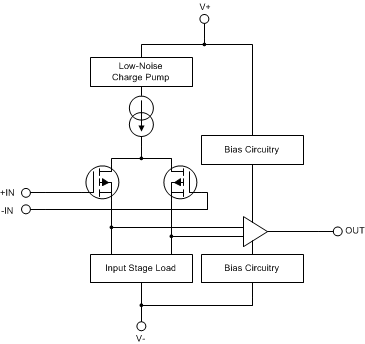
The TLVx369 family of operational amplifiers minimizes power consumption and operates on supply voltages as low as 1.8 V. The zero-crossover distortion circuitry enables high linearity over the full input common-mode range, achieving true rail-to-rail input from a 1.8-V to 5.5-V single supply.
7.2 Functional Block Diagram

7.3 Feature Description
7.3.1 Operating Voltage
The TLV369 series os op amps are fully specified and tested from 1.8 V to 5.5 V (±0.9 V to ±2.75 V). Parameters that vary significantly with supply voltage are described in the Typical Characteristics section.
7.3.2 Input Common-Mode Voltage Range
The TLV369 family is designed to eliminate the input offset transition region typically present in most rail-to-rail, complementary-stage operational amplifiers, allowing the TLV369 family of amplifiers to provide superior common-mode performance over the entire input range.
The input common-mode voltage range of the TLV369 family typically extends to each supply rail. CMRR is specified from the negative rail to the positive rail; see Figure 1, Normalized Offset Voltage vs Common-Mode Voltage.
7.3.3 Protecting Inputs from Overvoltage
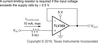
Input currents are typically 10 pA. However, large inputs (greater than 500 mV beyond the supply rails) can cause excessive current to flow in or out of the input pins. Therefore, in addition to keeping the input voltage between the supply rails, the input current must also be limited to less than 10 mA. This limiting is easily accomplished with an input resistor, as shown in Figure 14.
 Figure 14. Input Current Protection for Voltages That Exceed the Supply Voltage
7.4 Device Functional Modes
The TLV369 family has a single functional mode. These devices are powered on as long as the power-supply voltage is between 1.8 V (±0.9 V) and 5.5 V (±2.75 V).