ZHCSBX7D December 2013 – June 2015 TLV1701 , TLV1702 , TLV1704
PRODUCTION DATA.
- 1 特性
- 2 应用范围
- 3 说明
- 4 修订历史记录
- 5 Device Comparison
- 6 Pin Configuration and Functions
- 7 Specifications
- 8 Detailed Description
- 9 Applications and Implementation
- 10Power Supply Recommendations
- 11Layout
- 12器件和文档支持
- 13机械、封装和可订购信息
封装选项
机械数据 (封装 | 引脚)
散热焊盘机械数据 (封装 | 引脚)
- DGK|8
订购信息
8 Detailed Description
8.1 Overview
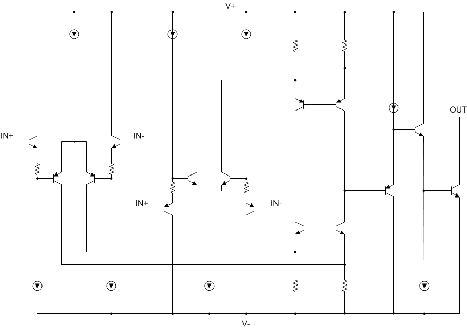
The TLV170x comparators features rail-to-rail input and output on supply voltages as high as 36 V. The rail-to-rail input stage enables detection of signals close to the supply and ground. The open collector configuration allows the device to be used in wired-OR configurations, such as a window comparator. A low supply current of 55 μA per channel with small, space-saving packages, makes these comparators versatile for use in a wide range of applications, from portable to industrial.
8.2 Functional Block Diagram

8.3 Feature Description
8.3.1 Comparator Inputs
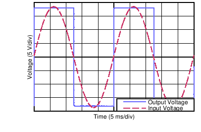
The TLV170x are rail-to-rail input comparators, with an input common-mode range that includes the supply rails. The TLV170x is designed to prevent phase inversion when the input pins exceed the supply voltage. Figure 18 shows the TLV170x response when input voltages exceed the supply, resulting in no phase inversion.
 Figure 18. No Phase Inversion: Comparator Response to Input Voltage
(Propagation Delay Included)
