ZHCSCU5A May 2014 – September 2014 TLC5958
PRODUCTION DATA.
- 1 特性
- 2 应用范围
- 3 说明
- 4 典型应用电路(多个菊花链 TLC5958)
- 5 修订历史记录
- 6 说明(继续)
- 7 Pin Configuration and Functions
- 8 Specifications
- 9 Parameter Measurement Information
-
10Detailed Description
- 10.1 Overview
- 10.2 Functional Block Diagram
- 10.3
Device Functional Modes
- 10.3.1 Brightness Control (BC) Function
- 10.3.2 Color Brightness Control (CC) Function
- 10.3.3 Select RIREF For a Given BC
- 10.3.4 Choosing BC/CC For a Different Application
- 10.3.5 LED Open Detection (LOD)
- 10.3.6 Power Save Mode (PSM)
- 10.3.7 Internal Pre-Charge FET
- 10.3.8 Thermal Shutdown (TSD)
- 10.3.9 IREF Resistor Short Protection (ISP)
- 10.3.10 Noise Reduction
- 11Application and Implementation
- 12Power Supply Recommendations
- 13Layout
- 14器件和文档支持
- 15机械封装和可订购信息
9 Parameter Measurement Information
9.1 Pin Equivalent Input and Output Schematic Diagrams
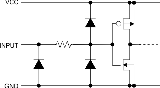 Figure 11. SIN, SCLK
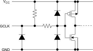 Figure 13. GCLK
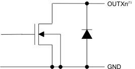
(1) X=R or G or B, n=0~15
Figure 15. OUTR0/G0/B0 Through OUTR15/G15/B15
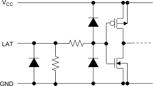 Figure 12. LAT
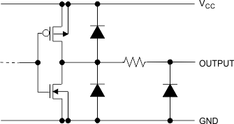 Figure 14. SOUT
9.1.1 Test Circuits
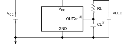
(1) CL includes measurement probe and jig capacitance.
(2) X=R or G or B, n=0~15
Figure 16. Rise Time and Fall Time Test Circuit for OUTXn
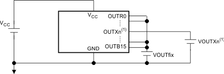
(1) X=R or G or B, n=0~15
Figure 18. Constant Current Test Circuit for OUTXn
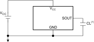
(1) CL includes measurement probe and jig capacitance.
Figure 17. Rise Time and Fall Time Test Circuit for SOUT
9.2 Timing Diagrams
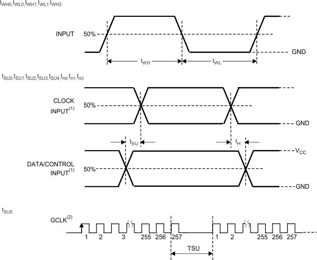
(1) Input pulse rise and fall time is 1~3ns
(2) 8 + 8 mode (SEL_PWM=0)
Figure 19. Timing Diagrams