SLDS157E February 2008 – December 2014 TLC59116
PRODUCTION DATA.
- 1 Features
- 2 Applications
- 3 Description
- 4 Revision History
- 5 Description (continued)
- 6 Pin Configuration and Functions
- 7 Specifications
- 8 Parameter Measurement Information
-
9 Detailed Description
- 9.1 Overview
- 9.2 Functional Block Diagram
- 9.3 Feature Description
- 9.4 Device Functional Modes
- 9.5
Register Maps
- 9.5.1 Mode Register 1 (MODE1)"SLEEP" to "OSC" in Mode Register 1 (MODE1) Table.
- 9.5.2 Mode Register 2 (MODE2)
- 9.5.3 Brightness Control Registers 0 to 15 (PWM0 to PWM15)
- 9.5.4 Group Duty Cycle Control Register (GRPPWM)
- 9.5.5 Group Frequency Register (GRPFREQ)
- 9.5.6 LED Driver Output State Registers 0 to 3 (LEDOUT0 to LEDOUT3)
- 9.5.7 I2C Bus Subaddress Registers 1 to 3 (SUBADR1 to SUBADR3)
- 9.5.8 LED All Call I2C Bus Address Register (ALLCALLADR)
- 9.5.9 Output Gain Control Register (IREF)
- 9.5.10 Error Flags Registers (EFLAG1, EFLAG2)
- 9.5.11 Control Register
-
10Application and Implementation
- 10.1 Application Information
- 10.2 Typical Application
- 11Power Supply Recommendations
- 12Layout
- 13Device and Documentation Support
- 14Mechanical, Packaging, and Orderable Information
封装选项
机械数据 (封装 | 引脚)
散热焊盘机械数据 (封装 | 引脚)
订购信息
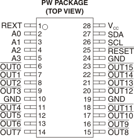
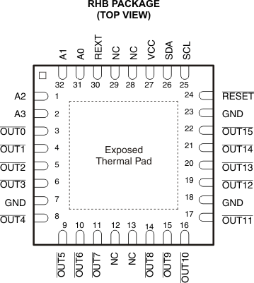
6 Pin Configuration and Functions
NC - No internal connection
If used, the exposed thermal pad must be connected as a secondary ground.
If used, the exposed thermal pad must be connected as a secondary ground.
Pin Functions
| PIN | I/O(1) | DESCRIPTION | ||
|---|---|---|---|---|
| NAME | PW NO. | RHB NO. | ||
| REXT | 1 | 30 | I | Input terminal used to connect an external resistor for setting up all output currents |
| A0 | 2 | 31 | I | Address input 0 |
| A1 | 3 | 32 | I | Address input 1 |
| A2 | 4 | 1 | I | Address input 2 |
| A3 | 5 | 2 | I | Address input 3 |
| OUT0 | 6 | 3 | O | Constant current output 0 |
| OUT1 | 7 | 4 | O | Constant current output 1 |
| OUT2 | 8 | 5 | O | Constant current output 2 |
| OUT3 | 9 | 6 | O | Constant current output 3 |
| GND | 10 | 7 | Ground | |
| OUT4 | 11 | 8 | O | Constant current output 4 |
| OUT5 | 12 | 9 | O | Constant current output 5 |
| OUT6 | 13 | 10 | O | Constant current output 6 |
| OUT7 | 14 | 11 | O | Constant current output 7 |
| OUT8 | 15 | 14 | O | Constant current output 8 |
| OUT9 | 16 | 15 | O | Constant current output 9 |
| OUT10 | 17 | 16 | O | Constant current output 10 |
| OUT11 | 18 | 17 | O | Constant current output 11 |
| GND | 19 | 18 | Ground | |
| OUT12 | 20 | 19 | O | Constant current output 12 |
| OUT13 | 21 | 20 | O | Constant current output 13 |
| OUT14 | 22 | 21 | O | Constant current output 14 |
| OUT15 | 23 | 22 | O | Constant current output 15 |
| GND | 24 | 23 | Ground | |
| RESET | 25 | 24 | I | Active-low reset input |
| SCL | 26 | 25 | I | Serial clock input |
| SDA | 27 | 26 | I/O | Serial data input/output |
| VCC | 28 | 27 | — | Power supply |
| NC | — | 12, 13, 28, 29 | — | No internal connection |
(1) I = input, O = output