SLDS157E February 2008 – December 2014 TLC59116
PRODUCTION DATA.
- 1 Features
- 2 Applications
- 3 Description
- 4 Revision History
- 5 Description (continued)
- 6 Pin Configuration and Functions
- 7 Specifications
- 8 Parameter Measurement Information
-
9 Detailed Description
- 9.1 Overview
- 9.2 Functional Block Diagram
- 9.3 Feature Description
- 9.4 Device Functional Modes
- 9.5
Register Maps
- 9.5.1 Mode Register 1 (MODE1)"SLEEP" to "OSC" in Mode Register 1 (MODE1) Table.
- 9.5.2 Mode Register 2 (MODE2)
- 9.5.3 Brightness Control Registers 0 to 15 (PWM0 to PWM15)
- 9.5.4 Group Duty Cycle Control Register (GRPPWM)
- 9.5.5 Group Frequency Register (GRPFREQ)
- 9.5.6 LED Driver Output State Registers 0 to 3 (LEDOUT0 to LEDOUT3)
- 9.5.7 I2C Bus Subaddress Registers 1 to 3 (SUBADR1 to SUBADR3)
- 9.5.8 LED All Call I2C Bus Address Register (ALLCALLADR)
- 9.5.9 Output Gain Control Register (IREF)
- 9.5.10 Error Flags Registers (EFLAG1, EFLAG2)
- 9.5.11 Control Register
-
10Application and Implementation
- 10.1 Application Information
- 10.2 Typical Application
- 11Power Supply Recommendations
- 12Layout
- 13Device and Documentation Support
- 14Mechanical, Packaging, and Orderable Information
封装选项
机械数据 (封装 | 引脚)
散热焊盘机械数据 (封装 | 引脚)
订购信息
12 Layout
12.1 Layout Guidelines
The I2C signals (SDA / SCL) should be kept away from potential noise sources.
The traces carrying power through the LEDS should be wide enough to the handle necessary current.
All LED current passes through the device and into the ground node. There must be a strong connection between the device ground and the circuit board ground. For the RHB package, the thermal pad should be connected to ground to help dissipate heat.
12.2 Layout Example
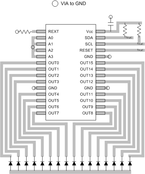 Figure 23. PW Layout Example
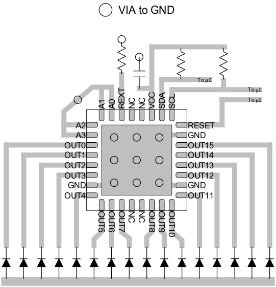 Figure 24. RHB Layout Example
The thermal relief vias are connected to the power pad of the RHB package shown in Figure 24.
12.3 Thermal Considerations
The maximum IC junction temperature should be restricted to 150°C under normal operating conditions. To calculate the maximum allowable dissipation, PD(max) for a given ambient temperature, use the following equation as a guideline:
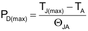
where
- PD(max) = maximum allowable power dissipation
- TJ(max) = maximum allowable junction temperature (150°C for the TLC59116)
- TA = ambient temperature of the device
- ΘJA = junction to air thermal impedance.
See Thermal Information section. This parameter is highly dependent upon board layout.
Power dissipation in the device is determined by the LED current and the voltage at the OUTx pins. For example, if the LED current is 50 mA continuous through each channel and the output voltage is 1 V on each channel, then the total power dissipation is 50 mA x 1 V x 16 ch = 0.8 W