SLVS529D April 2004 – January 2015 TL1431-EP
PRODUCTION DATA.
- 1 Features
- 2 Applications
- 3 Description
- 4 Simplified Schematic
- 5 Revision History
- 6 Pin Configuration and Functions
- 7 Specifications
- 8 Parameter Measurement Information
- 9 Detailed Description
- 10Application and Implementation
- 11Power Supply Recommendations
- 12Layout
- 13Device and Documentation Support
- 14Mechanical, Packaging, and Orderable Information
1 Features
- 0.4% Initial Voltage Tolerance
- 0.2-Ω Typical Output Impedance
- Fast Turnon: 500 ns
- Sink Current Capability: 1 to 100 mA
- Low Reference Current (REF)
- Adjustable Output Voltage: VI(ref) to 36 V
- Supports Defense, Aerospace, and Medical Applications
- Controlled Baseline
- One Assembly and Test Site
- One Fabrication Site
- Available in Military (–55°C to 125°C) Temperature Range
- Extended Product Life Cycle
- Extended Product-Change Notification
- Product Traceability
2 Applications
- Shunt Regulators
- Temperature-Compensated Comparators
- PWM Converter Reference
- Photodiode Reference Drivers
- Precision Current Limiters
- Precision Current Sink
3 Description
The TL1431-EP device is a precision-programmable reference with specified thermal stability over the military temperature range. The output voltage can be set to any value from VI(ref) (approximately 2.5 V) to 36 V with two external resistors (see Figure 21). This device has a typical output impedance of 0.2 Ω. Active output circuitry provides a very sharp turnon characteristic, making the device an excellent replacement for Zener diodes and other types of references in applications such as onboard regulation, adjustable power supplies, and switching power supplies.
Device Information(1)
| PART NUMBER | PACKAGE | BODY SIZE (NOM) |
|---|---|---|
| TL1431-EP | SOIC (8) | 3.91 mm × 4.90 mm |
- For all available packages, see the orderable addendum at the end of the data sheet.
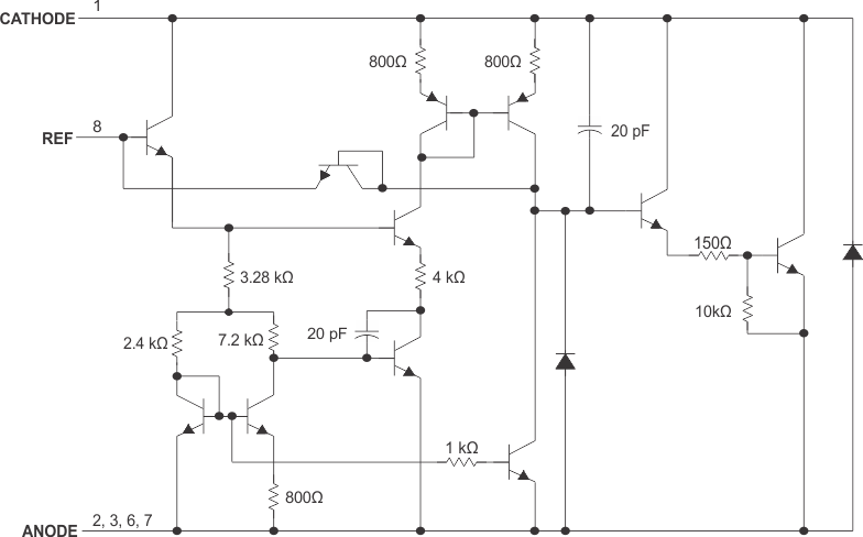
4 Simplified Schematic
Symbol