ZHCSGR5 September 2017 TIC12400
PRODUCTION DATA.
- 1 特性
- 2 应用
- 3 说明
- 4 修订历史记录
- 5 Pin Configuration and Functions
- 6 Specifications
- 7 Parameter Measurement Information
-
8 Detailed Description
- 8.1 Overview
- 8.2 Functional Block Diagram
- 8.3
Feature Description
- 8.3.1 VS Pin
- 8.3.2 VDD Pin
- 8.3.3 Device Initialization
- 8.3.4 Device Trigger
- 8.3.5 Device Reset
- 8.3.6 VS Under-Voltage (UV) Condition
- 8.3.7 VS Over-Voltage (OV) Condition
- 8.3.8 Switch inputs Settings
- 8.3.9 Interrupt Generation and INT Assertion
- 8.3.10 Temperature Monitor
- 8.3.11 Parity Check And Parity Generation
- 8.3.12 Cyclic Redundancy Check (CRC)
- 8.4 Device Functional Modes
- 8.5 Programming
- 8.6
Register Maps
- 8.6.1 DEVICE_ID register (Offset = 1h) [reset = 20h]
- 8.6.2 INT_STAT Register (Offset = 2h) [reset = 1h]
- 8.6.3 CRC Register (Offset = 3h) [reset = FFFFh]
- 8.6.4 IN_STAT_MISC Register (Offset = 4h) [reset = 0h]
- 8.6.5 IN_STAT_COMP Register (Offset = 5h) [reset = 0h]
- 8.6.6 IN_STAT_ADC0 Register (Offset = 6h) [reset = 0h]
- 8.6.7 IN_STAT_ADC1 Register (Offset = 7h) [reset = 0h]
- 8.6.8 IN_STAT_MATRIX0 Register (Offset = 8h) [reset = 0h]
- 8.6.9 IN_STAT_MATRIX1 Register (Offset = 9h) [reset = 0h]
- 8.6.10 ANA_STAT0 Register (Offset = Ah) [reset = 0h]
- 8.6.11 ANA_STAT1 Register (Offset = Bh) [reset = 0h]
- 8.6.12 ANA_STAT2 Register (Offset = Ch) [reset = 0h]
- 8.6.13 ANA_STAT3 Register (Offset = Dh) [reset = 0h]
- 8.6.14 ANA_STAT4 Register (Offset = Eh) [reset = 0h]
- 8.6.15 ANA_STAT5 Register (Offset = Fh) [reset = 0h]
- 8.6.16 ANA_STAT6 Register (Offset = 10h) [reset = 0h]
- 8.6.17 ANA_STAT7 Register (Offset = 11h) [reset = 0h]
- 8.6.18 ANA_STAT8 Register (Offset = 12h) [reset = 0h]
- 8.6.19 ANA_STAT9 Register (Offset = 13h) [reset = 0h]
- 8.6.20 ANA_STAT10 Register (Offset = 14h) [reset = 0h]
- 8.6.21 ANA_STAT11 Register (Offset = 15h) [reset = 0h]
- 8.6.22 ANA_STAT12 Register (Offset = 16h) [reset = 0h]
- 8.6.23 CONFIG Register (Offset = 1Ah) [reset = 0h]
- 8.6.24 IN_EN Register (Offset = 1Bh) [reset = 0h]
- 8.6.25 CS_SELECT Register (Offset = 1Ch) [reset = 0h]
- 8.6.26 WC_CFG0 Register (Offset = 1Dh) [reset = 0h]
- 8.6.27 WC_CFG1 Register (Offset = 1Eh) [reset = 0h]
- 8.6.28 CCP_CFG0 Register (Offset = 1Fh) [reset = 0h]
- 8.6.29 CCP_CFG1 Register (Offset = 20h) [reset = 0h]
- 8.6.30 THRES_COMP Register (Offset = 21h) [reset = 0h]
- 8.6.31 INT_EN_COMP1 Register (Offset = 22h) [reset = 0h]
- 8.6.32 INT_EN_COMP2 Register (Offset = 23h) [reset = 0h]
- 8.6.33 INT_EN_CFG0 Register (Offset = 24h) [reset = 0h]
- 8.6.34 INT_EN_CFG1 Register (Offset = 25h) [reset = 0h]
- 8.6.35 INT_EN_CFG2 Register (Offset = 26h) [reset = 0h]
- 8.6.36 INT_EN_CFG3 Register (Offset = 27h) [reset = 0h]
- 8.6.37 INT_EN_CFG4 Register (Offset = 28h) [reset = 0h]
- 8.6.38 THRES_CFG0 Register (Offset = 29h) [reset = 0h]
- 8.6.39 THRES_CFG1 Register (Offset = 2Ah) [reset = 0h]
- 8.6.40 THRES_CFG2 Register (Offset = 2Bh) [reset = 0h]
- 8.6.41 THRES_CFG3 Register (Offset = 2Ch) [reset = X]
- 8.6.42 THRES_CFG4 Register (Offset = 2Dh) [reset = X]
- 8.6.43 THRESMAP_CFG0 Register (Offset = 2Eh) [reset = 0h]
- 8.6.44 THRESMAP_CFG1 Register (Offset = 2Fh) [reset = 0h]
- 8.6.45 THRESMAP_CFG2 Register (Offset = 30h) [reset = 0h]
- 8.6.46 Matrix Register (Offset = 31h) [reset = 0h]
- 8.6.47 Mode Register (Offset = 32h) [reset = 0h]
- 8.7 Programming Guidelines
- 9 Application and Implementation
- 10Power Supply Recommendations
- 11Layout
- 12器件和文档支持
- 13机械、封装和可订购信息
10 Power Supply Recommendations
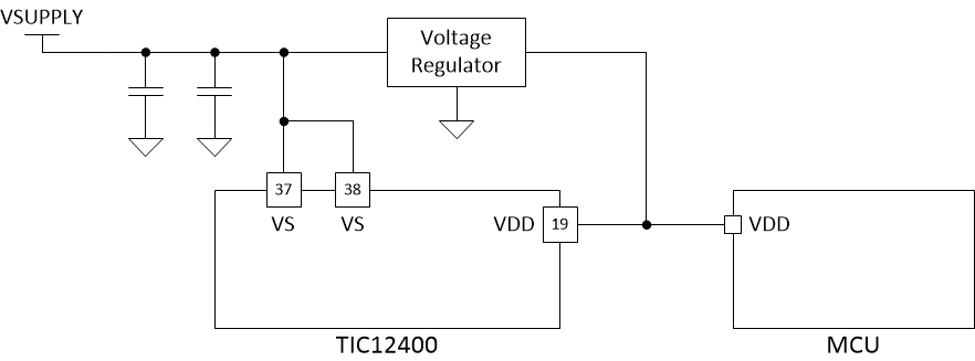
There are two supply input pins for the TIC12400: VS and VDD. VS is the main power supply for the entire chip and is essential for all critical functions of the device. The TIC12400 is designed to operate with VS ranging from 6.5 V to 35 V. The VDD supply is used to determine the logic level on the SPI communication interface, source the current for the SO driver, and sets the pull-up voltage for the CS pin. It can also be used as a possible external pull-up supply for the /INT pinas an alternative to the VS supply and it shall be connected to a 3 V to 5.5 V logic supply. Removing VDD from the device disables SPI communications, but does not impact normal operation of the device.
To improve stability of the supply inputs, some decoupling capacitors are recommended on the PCB. Figure 87 shows an example on the on-board power supply decoupling scheme. The supply voltage (VSUPPLY) is decoupled on the Electronic Control Unit (ECU) board using a large decoupling capacitor (CBUFF). The diode is installed to prevent damage to the internal system under reversed supply condition. CVS shall be installed closed to the TIC12400 for best decoupling performance. The voltage regulator provides a regulated voltage for the digital potion of the device and for the local microcontroller and its output is decoupled with CDECOUPLE. Table 61 lists recommended values for each individual decoupling capacitor shown in the system diagram.
Table 61. Decoupling Capacitor Recommendations
| Component | Value |
|---|---|
| CBUFF | 100 μF, 50V rated, ±20% |
| CVSUPPLY | 100 nF, 50 V rated, ±10%; X7R |
| CVS | 100 nF, 50 V rated |
| CDECOUPLE | 100 nF ~ 1 μF |
 Figure 87. Recommended Power Supply Decoupling