ZHCSEK0A November 2015 – November 2015 THS4541-Q1
PRODUCTION DATA.
- 1 特性
- 2 应用
- 3 说明
- 4 修订历史记录
- 5 Device Family Comparison
- 6 Pin Configuration and Functions
- 7 Specifications
-
8 Parameter Measurement Information
- 8.1 Example Characterization Circuits
- 8.2 Frequency-Response Shape Factors
- 8.3 I/O Headroom Considerations
- 8.4 Output DC Error and Drift Calculations and the Effect of Resistor Imbalances
- 8.5 Noise Analysis
- 8.6 Factors Influencing Harmonic Distortion
- 8.7 Driving Capacitive Loads
- 8.8 Thermal Analysis
-
9 Detailed Description
- 9.1 Overview
- 9.2 Functional Block Diagram
- 9.3 Feature Description
- 9.4
Device Functional Modes
- 9.4.1
Operation from Single-Ended Sources to Differential Outputs
- 9.4.1.1 AC-Coupled Signal Path Considerations for Single-Ended Input to Differential Output Conversion
- 9.4.1.2 DC-Coupled Input Signal Path Considerations for Single-Ended to Differential Conversion
- 9.4.1.3 Resistor Design Equations for the Single-Ended to Differential Configuration of the FDA
- 9.4.1.4 Input Impedance for the Single-Ended to Differential FDA Configuration
- 9.4.2 Differential-Input to Differential-Output Operation
- 9.4.1
Operation from Single-Ended Sources to Differential Outputs
- 10Application and Implementation
- 11Power-Supply Recommendations
- 12Layout
- 13器件和文档支持
- 14机械、封装和可订购信息
7 Specifications
7.1 Absolute Maximum Ratings
over operating free-air temperature range (unless otherwise noted)(1)| MIN | MAX | UNIT | ||
|---|---|---|---|---|
| Voltage | Supply voltage, (Vs+) – Vs– | 5.5 | V | |
| Input/output voltage range | (Vs–) – 0.5 | (Vs+) + 0.5 | V | |
| Differential input voltage | ±1 | V | ||
| Current | Continuous input current | ±20 | mA | |
| Continuous output current | ±80 | mA | ||
| Continuous power dissipation | See Thermal Information table and Thermal Analysis section | |||
| Temperature | Maximum junction temperature | 150 | °C | |
| Operating free-air temperature range | –40 | 125 | °C | |
| Storage temperature, Tstg | –65 | 150 | °C | |
(1) Stresses beyond those listed under Absolute Maximum Ratings may cause permanent damage to the device. These are stress ratings only, which do not imply functional operation of the device at these or any other conditions beyond those indicated under Recommended Operating Conditions. Exposure to absolute-maximum-rated conditions for extended periods may affect device reliability.
7.2 ESD Ratings
| VALUE | UNIT | |||
|---|---|---|---|---|
| V(ESD) | Electrostatic discharge | Human-body model (HBM), per AEC Q100-002(1) | ±2000 | V |
| Charged-device model (CDM), per AEC Q100-011 | ±1000 | |||
(1) AEC Q100-002 indicates that HBM stressing shall be in accordance with the ANSI/ESDA/JEDEC JS-001 specification.
7.3 Recommended Operating Conditions
over operating free-air temperature range (unless otherwise noted)| MIN | NOM | MAX | UNIT | ||
|---|---|---|---|---|---|
| Vs+ | Single-supply voltage | 2.7 | 5 | 5.4 | V |
| TA | Ambient temperature | –40 | 25 | 125 | °C |
7.4 Thermal Information
| THERMAL METRIC(1) | THS4541-Q1 | UNIT | |
|---|---|---|---|
| RGT (VQFN) | |||
| 16 PINS | |||
| RθJA | Junction-to-ambient thermal resistance | 52 | °C/W |
| RθJC(top) | Junction-to-case (top) thermal resistance | 69 | °C/W |
| RθJB | Junction-to-board thermal resistance | 25 | °C/W |
| ψJT | Junction-to-top characterization parameter | 2.7 | °C/W |
| ψJB | Junction-to-board characterization parameter | 25 | °C/W |
| RθJC(bot) | Junction-to-case (bottom) thermal resistance | 9.3 | °C/W |
(1) For more information about traditional and new thermal metrics, see the Semiconductor and IC Package Thermal Metrics application report, SPRA953.
7.5 Electrical Characteristics: (Vs+) – Vs– = 5 V
At TA ≈ 25°C, Vocm = open (defaults midsupply), VOUT = 2 VPP, Rf = 402 Ω, Rload = 499 Ω, 50-Ω input match, G = 2 V/V, single-ended input, differential output, and PD = +Vs, unless otherwise noted. See Figure 61 for an AC-coupled gain of a 2-V/V test circuit, and Figure 63 for a DC-coupled gain of a 2-V/V test circuit.| PARAMETER | TEST CONDITIONS | MIN | TYP | MAX | UNIT | TEST LEVEL(1) |
|||
|---|---|---|---|---|---|---|---|---|---|
| AC PERFORMANCE | |||||||||
| Small-signal bandwidth | Vout = 100 mVPP, G = 1 | 620 | MHz | C | |||||
| Vout = 100 mVPP, G = 2 (see Figure 61) | 500 | MHz | C | ||||||
| Vout = 100 mVPP, G = 5 | 210 | MHz | C | ||||||
| Vout = 100 mVPP, G = 10 | 125 | MHz | C | ||||||
| Gain-bandwidth product | Vout = 100 mVPP, G = 20 | 850 | MHz | C | |||||
| Large-signal bandwidth | Vout = 2 VPP, G = 2 (see Figure 61) | 340 | MHz | C | |||||
| Bandwidth for 0.1-dB flatness | Vout = 2 VPP, G = 2 (see Figure 61) | 100 | MHz | C | |||||
| Slew rate(2) | Vout = 2-VPP, FPBW (see Figure 61) | 1500 | V/µs | C | |||||
| Rise/fall time | Vout = 2-V step, G = 2 input ≤ 0.3 ns tr
(see Figure 63) |
1.4 | ns | C | |||||
| Settling time | To 1%, Vout = 2-V step, tr = 2 ns, G = 2 (seeFigure 63) | 4 | ns | C | |||||
| To 0.1%,Vout = 2-V step, tr = 2 ns, G = 2 (see Figure 63) | 8 | ns | C | ||||||
| Overshoot and undershoot | Vout = 2-V step G = 2, input ≤ 0.3 ns tr
(see Figure 63) |
10% | C | ||||||
| 100-kHz harmonic distortion | Vout = 2 VPP, G = 2, HD2 (see Figure 61) | –140 | dBc | C | |||||
| Vout = 2 VPP, G = 2, HD3 (see Figure 61) | –140 | dBc | C | ||||||
| 10-MHz harmonic distortion | Vout = 2 VPP, G = 2, HD2 (see Figure 61) | –95 | dBc | C | |||||
| Vout = 2 VPP, G = 2, HD3 (see Figure 61) | –90 | dBc | C | ||||||
| 2nd-order intermodulation distortion | f = 10 MHz, 100-kHz tone spacing, Vout envelope = 2 VPP (1 VPP per tone) (see Figure 61) |
–90 | dBc | C | |||||
| 3rd-order intermodulation distortion | f = 10 MHz, 100-kHz tone spacing, Vout envelope = 2 VPP (1 VPP per tone) (see Figure 61) |
–85 | dBc | C | |||||
| Input voltage noise | f > 100 kHz | 2.2 | nV/√Hz | C | |||||
| Input current noise | f > 1 MHz | 1.9 | pA/√Hz | C | |||||
| Overdrive recovery time | 2x output overdrive, either polarity | 20 | ns | C | |||||
| Closed-loop output impedance | f = 10 MHz (differential) | 0.1 | Ω | C | |||||
| DC PERFORMANCE | |||||||||
| AOL | Open-loop voltage gain | 100 | 119 | dB | A | ||||
| Input-referred offset voltage | TA = 25°C | –450 | ±100 | 450 | µV | A | |||
| TA = 0°C to 70°C | –600 | ±100 | 600 | µV | B | ||||
| TA = –40°C to +85°C | –700 | ±100 | 700 | µV | B | ||||
| TA = –40°C to +125°C | –850 | ±100 | 850 | µV | B | ||||
| Input offset voltage drift(3) | TA = –40°C to +125°C | –2.4 | ±0.5 | 2.4 | µV/°C | B | |||
| Input bias current (positive out of node) |
TA = 25°C | 4.3 | 10 | 13 | µA | A | |||
| TA = 0°C to 70°C | 4.3 | 11 | 13.5 | µA | B | ||||
| TA = –40°C to +85°C | 4.3 | 12 | 14 | µA | B | ||||
| TA = –40°C to +125°C | 4.3 | 12 | 14.5 | µA | B | ||||
| Input bias current drift(3) | TA = –40°C to +125°C | 6 | 15 | nA/°C | B | ||||
| Input offset current | TA = 25°C | –500 | ±150 | 500 | nA | A | |||
| TA = 0°C to 70°C | –550 | ±150 | 550 | nA | B | ||||
| TA = –40°C to +85°C | –580 | ±150 | 580 | nA | B | ||||
| TA = –40°C to +125°C | –620 | ±150 | 620 | nA | B | ||||
| Input offset current drift(3) | TA = –40°C to +125°C | –1.3 | ±0.3 | 1.3 | nA/°C | B | |||
| INPUT | |||||||||
| Common-mode input low | < 3-dB degradation in CMRR from midsupply | TA = 25°C | (Vs–) – 0.2 | (Vs–) – 0.1 | V | A | |||
| TA = –40°C to +125°C | (Vs–) – 0.1 | Vs– | V | B | |||||
| Common-mode input high | < 3-dB degradation in CMRR from midsupply | TA = 25°C | (Vs+) – 1.3 | (Vs+) –1.2 | V | A | |||
| TA = –40°C to +125°C | (Vs+) – 1.3 | V | B | ||||||
| Common-mode rejection ratio | Input pins at ((Vs+) – Vs–) / 2 | 85 | 100 | dB | A | ||||
| Input impedance differential mode | Input pins at ((Vs+) – Vs–) / 2 | 110 || 0.85 | kΩ || pF | C | |||||
| OUTPUT | |||||||||
| Output voltage low | TA = 25°C | (Vs–) + 0.2 | (Vs–) + 0.25 | V | A | ||||
| TA = –40°C to +125°C | (Vs–) + 0.2 | (Vs–) + 0.25 | V | B | |||||
| Output voltage high | TA = 25°C | (Vs+) – 0.25 | (Vs+) – 0.2 | V | A | ||||
| TA = –40°C to +125°C | (Vs+) – 0.25 | (Vs+) – 0.2 | V | B | |||||
| Output current drive | TA = 25°C | ±75 | ±100 | mA | A | ||||
| TA = –40°C to +125°C | ±75 | mA | B | ||||||
| POWER SUPPLY | |||||||||
| Specified operating voltage | 2.7 | 5 | 5.4 | V | B | ||||
| Quiescent operating current | TA = 25°C, Vs+ = 5 V | 9.7 | 10.1 | 10.5 | mA | A | |||
| TA = –40°C to +125°C | 9.4 | 10.1 | 11 | mA | B | ||||
| ±PSRR | Power-supply rejection ratio | Either supply pin to differential Vout | 85 | 100 | dB | A | |||
| POWER DOWN | |||||||||
| Enable voltage threshold | (Vs–) + 1.7 | V | A | ||||||
| Disable voltage threshold | (Vs–) + 0.7 | V | A | ||||||
| Disable pin bias current | PD = Vs– → Vs+ | 20 | 50 | nA | B | ||||
| Power-down quiescent current | PD = (Vs–) + 0.7 V | 6 | 30 | µA | A | ||||
| PD = Vs– | 2 | 8 | µA | A | |||||
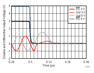
| Turn-on time delay | Time from PD = low to Vout = 90% of final value | 100 | ns | C | |||||
| Turn-off time delay | Time from PD = low to Vout = 10% of final value | 60 | ns | C | |||||
| OUTPUT COMMON-MODE VOLTAGE CONTROL(4) | |||||||||
| Small-signal bandwidth | Vocm = 100 mVPP | 150 | MHz | C | |||||
| Slew rate(2) | Vocm = 2-V step | 400 | V/µs | C | |||||
| Gain | 0.975 | 0.982 | 0.995 | V/V | A | ||||
| Input bias current | Considered positive out of node | –0.7 | 0.1 | 0.7 | µA | A | |||
| Input impedance | Vocm input driven to ((Vs+) – Vs–) / 2 | 47 || 1.2 | kΩ || pF | C | |||||
| Default voltage offset from ((Vs+) – Vs–) / 2 |
Vocm pin open | –40 | ±8 | 40 | mV | A | |||
| CM Vos | Common-mode offset voltage | Vocm input driven to ((Vs+) – Vs–) / 2 | TA = 25°C | –5 | ±2 | 5 | mV | A | |
| TA = 0°C to 70°C | –6 | ±2 | 5.8 | mV | B | ||||
| TA = –40°C to +85°C | –6.2 | ±2 | 6.2 | mV | B | ||||
| TA = –40°C to +125°C | –7 | ±2 | 7.08 | mV | B | ||||
| Common-mode offset voltage drift(3) | Vocm input driven to ((Vs+) – Vs–) / 2 | –20 | ±4 | +20 | µV/°C | B | |||
| Common-mode loop supply headroom to negative supply | < ±12-mV shift from midsupply CM Vos | TA = 25°C | 0.88 | V | A | ||||
| TA = 0°C to 70°C | 0.91 | V | B | ||||||
| TA = –40°C to +85°C | 0.94 | V | B | ||||||
| TA = –40°C to +125°C | 0.94 | V | B | ||||||
| Common-mode loop supply headroom to positive supply | < ±12-mV shift from midsupply CM Vos | TA = 25°C | 1.1 | V | A | ||||
| TA = 0°C to 70°C | 1.15 | V | B | ||||||
| TA = –40°C to +85°C | 1.2 | V | B | ||||||
| TA = –40°C to +125°C | 1.2 | V | B | ||||||
(1) Test levels (all values set by characterization and simulation): (A) 100% tested at TA ≈ 25°C; over temperature limits by characterization and simulation. (B) Not tested in production; limits set by characterization and simulation. (C) Typical value only for information.
(2) This slew rate is the average of the rising and falling time estimated from the large-signal bandwidth as: (VP / √2) · 2π · f–3dB.
(3) Input offset voltage drift, input bias current drift, input offset current drift, and Vocm drift are average values calculated by taking data at the at the maximum-range ambient-temperature end points, computing the difference, and dividing by the temperature range. Maximum drift set by distribution of a large sampling of devices. Drift is not specified by test or QA sample test.
(4) Specifications are from the input Vocm pin to the differential output average voltage.
7.6 Electrical Characteristics: (Vs+) – Vs– = 3 V
At TA ≈ 25°C, Vocm = open (defaults midsupply), VOUT = 2 VPP, Rf = 402 Ω, Rload = 499 Ω, 50-Ω input match, G = 2 V/V, single-ended input, differential output, and PD = +Vs, unless otherwise noted. See Figure 61 for an AC-coupled gain of a 2-V/V test circuit, and Figure 63 for a DC-coupled gain of a 2-V/V test circuit.| PARAMETER | TEST CONDITIONS | MIN | TYP | MAX | UNIT | TEST LEVEL(1) |
|||
|---|---|---|---|---|---|---|---|---|---|
| AC PERFORMANCE | |||||||||
| Small-signal bandwidth | Vout = 100 mVPP, G = 1 | 600 | MHz | C | |||||
| Vout = 100 mVPP, G = 2 (see Figure 61) | 500 | MHz | C | ||||||
| Vout = 100 mVPP, G = 5 | 200 | MHz | C | ||||||
| Vout = 100 mVPP, G = 10 | 120 | MHz | C | ||||||
| Gain-bandwidth product | Vout = 100 mVPP, G = 20 | 850 | MHz | C | |||||
| Large-signal bandwidth | Vout = 2 VPP, G = 2 (see Figure 61) | 300 | MHz | C | |||||
| Bandwidth for 0.1-dB flatness | Vout = 2 VPP, G = 2 (see Figure 61) | 90 | MHz | C | |||||
| Slew rate(2) | Vout = 2-V step, FPBW (see Figure 61) | 1300 | V/µs | C | |||||
| Rise/fall time | Vout = 2-V step, G = 2, input ≤ 0.3 ns tr
(see Figure 63) |
1.8 | ns | C | |||||
| Settling time | To 1%, Vout = 2-V step, tr = 2 ns, G = 2 (see Figure 63) |
5 | ns | C | |||||
| To 0.1%, Vout = 2-V step, tr = 2 ns, G = 2 (see Figure 63) |
8 | ns | C | ||||||
| Overshoot and undershoot | Vout = 2-V step G = 2, input ≤ 0.3 ns tr
(see Figure 63) |
10% | C | ||||||
| 100-kHz harmonic distortion | Vout = 2 VPP, G = 2, HD2 (see Figure 61) | –140 | dBc | C | |||||
| Vout = 2 VPP, G = 2, HD3 (see Figure 61) | –140 | dBc | C | ||||||
| 10-MHz harmonic distortion | Vout = 2 VPP, G = 2, HD2 (see Figure 61) | –92 | dBc | C | |||||
| Vout = 2 VPP, G = 2, HD3 (see Figure 61) | –89 | dBc | C | ||||||
| 2nd-order intermodulation distortion | f = 10 MHz, 100-kHz tone spacing, Vout envelope = 2 VPP (1 VPP per tone) (see Figure 61) |
–89 | dBc | C | |||||
| 3rd-order intermodulation distortion | f = 10 MHz, 100-kHz tone spacing, Vout envelope = 2 VPP (1 VPP per tone) (see Figure 61) |
–87 | dBc | C | |||||
| Input voltage noise | f > 100 kHz | 2.2 | nV/√Hz | C | |||||
| Input current noise | f > 1 MHz | 1.9 | pA/√Hz | C | |||||
| Overdrive recovery time | 2X output overdrive, either polarity | 20 | ns | C | |||||
| Closed-loop output impedance | f = 10 MHz (differential) | 0.1 | Ω | C | |||||
| DC PERFORMANCE | |||||||||
| AOL | Open-loop voltage gain | 100 | 119 | dB | A | ||||
| Input-referred offset voltage | TA = 25°C | –450 | ±100 | 400 | µV | A | |||
| TA = 0°C to 70°C | –600 | ±100 | 600 | µV | B | ||||
| TA = –40°C to +85°C | –700 | ±100 | 700 | µV | B | ||||
| TA = –40°C to +125°C | –850 | ±100 | 850 | µV | B | ||||
| Input offset voltage drift(3) | TA = –40°C to +125°C | –2.4 | ±0.5 | 2.4 | µV/°C | B | |||
| Input bias current (positive out of node) |
TA = 25°C | 4.1 | 9 | 12 | µA | A | |||
| TA = 0°C to 70°C | 4.1 | 9 | 12.5 | µA | B | ||||
| TA = –40°C to +85°C | 4.1 | 9 | 13 | µA | B | ||||
| TA = –40°C to +125°C | 4.1 | 9 | 13.5 | µA | B | ||||
| Input bias current drift(3) | TA = –40°C to +125°C | –5 | 15 | nA/°C | B | ||||
| Input offset current | TA = 25°C | –500 | ±150 | 500 | nA | A | |||
| TA = 0°C to 70°C | –550 | ±150 | 550 | nA | B | ||||
| TA = –40°C to +85°C | –580 | ±150 | 580 | nA | B | ||||
| TA = –40°C to +125°C | –620 | ±150 | 620 | nA | B | ||||
| Input offset current drift(3) | TA = –40°C to +125°C | –1.3 | ±0.3 | 1.3 | nA/°C | B | |||
| INPUT | |||||||||
| Common-mode input low | < 3-dB degradation in CMRR from midsupply | TA = 25°C | (Vs–) – 0.2 | (Vs–) – 0.1 | V | A | |||
| TA = –40°C to +125°C | (Vs–) – 0.1 | Vs– | V | B | |||||
| Common-mode input high | < 3-dB degradation in CMRR from midsupply | TA = 25°C | (Vs+) – 1.3 | (Vs+) –1.2 | V | A | |||
| TA = –40°C to +125°C | (Vs+) – 1.3 | V | B | ||||||
| Common-mode rejection ratio | Input pins at ((Vs+) – Vs–) / 2 | 85 | 100 | dB | A | ||||
| Input impedance differential mode | Input pins at ((Vs+) – Vs–) / 2 | 110 || 0.85 | kΩ || pF | C | |||||
| OUTPUT | |||||||||
| Output voltage low | TA = 25°C | (Vs–) + 0.2 | (Vs–) + 0.25 | V | A | ||||
| TA = –40°C to +125°C | (Vs–) + 0.2 | (Vs–) + 0.25 | V | B | |||||
| Output voltage high | TA = 25°C | (Vs+) – 0.25 | (Vs+) – 0.2 | V | A | ||||
| TA = –40°C to +125°C | (Vs+) – 0.25 | (Vs+) – 0.2 | V | B | |||||
| Output current drive | TA = 25°C | ±55 | ±60 | mA | A | ||||
| TA = –40°C to +125°C | ±55 | mA | B | ||||||
| POWER SUPPLY | |||||||||
| Specified operating voltage | 2.7 | 3 | 5.4 | V | B | ||||
| Quiescent operating current | TA = 25°C, Vs+ = 3V | 9.3 | 9.7 | 10.1 | mA | A | |||
| TA = –40°C to +125°C | 9 | 9.7 | 10.6 | mA | B | ||||
| ±PSRR | Power-supply rejection ratio | Either supply pin to differential Vout | 85 | 100 | dB | A | |||
| POWER DOWN | |||||||||
| Enable voltage threshold | (Vs–) + 1.7 | V | A | ||||||
| Disable voltage threshold | (Vs–) + 0.7 | V | A | ||||||
| Disable pin bias current | PD = Vs– → Vs+ | 20 | 50 | nA | B | ||||
| Power-down quiescent current | PD = (Vs–) + 0.7 V | 2 | 30 | µA | A | ||||
| PD = Vs– | 1.0 | 8.0 | µA | A | |||||
| Turn-on time delay | Time from PD = low to Vout = 90% of final value | 100 | ns | C | |||||
| Turn-off time delay | Time from PD = low to Vout = 10% of final value | 60 | ns | C | |||||
| OUTPUT COMMON-MODE VOLTAGE CONTROL(4) | |||||||||
| Small-signal bandwidth | Vocm = 100 mVPP | 140 | MHz | C | |||||
| Slew rate(2) | Vocm = 1-V step | 350 | V/µs | C | |||||
| Gain | 0.975 | 0.987 | 0.990 | V/V | A | ||||
| Input bias current | Considered positive out of node | –0.7 | 0.1 | 0.7 | µA | A | |||
| Input impedance | Vocm input driven to ((Vs+) – Vs–) / 2 | 47 || 1.2 | kΩ || pF | C | |||||
| Default voltage offset from ((Vs+) – Vs–) / 2 |
Vocm pin open | –40 | ±10 | 40 | mV | A | |||
| CM Vos | Common-mode offset voltage | Vocm input driven to ((Vs+) – Vs–) / 2 | TA = 25°C | –5 | ±2 | 5 | mV | A | |
| TA = 0°C to 70°C | –5.8 | ±2 | 5.8 | mV | B | ||||
| TA = –40°C to +85°C | –6.2 | ±2 | 6.2 | mV | B | ||||
| TA = –40°C to +125°C | –7 | ±2 | 7 | mV | B | ||||
| Common-mode offset voltage drift(3) | Vocm input driven to ((Vs+) – Vs–) / 2 | –20 | ±4 | 20 | µV/°C | B | |||
| Common-mode loop supply headroom to negative supply | < ±12-mV shift from midsupply CM Vos | TA = 25°C | 0.88 | V | A | ||||
| TA = 0°C to 70°C | 0.91 | V | B | ||||||
| TA = –40°C to +85°C | 0.94 | V | B | ||||||
| TA = –40°C to +125°C | 0.94 | V | B | ||||||
| Common-mode loop supply headroom to positive supply | < ±12-mV shift from midsupply CM Vos | TA = 25°C | 1.1 | V | A | ||||
| TA = 0°C to 70°C | 1.15 | V | B | ||||||
| TA = –40°C to +85°C | 1.2 | V | B | ||||||
| TA = –40°C to +125°C | 1.2 | V | B | ||||||
(1) Test levels (all values set by characterization and simulation): (A) 100% tested at TA ≈ 25°C; over temperature limits by characterization and simulation. (B) Not tested in production; limits set by characterization and simulation. (C) Typical value only for information.
(2) This slew rate is the average of the rising and falling time estimated from the large-signal bandwidth as: (VP / √2) · 2π · f–3dB.
(3) Input offset voltage drift, input bias current drift, input offset current drift, and Vocm drift are average values calculated by taking data at the at the maximum-range ambient-temperature end points, computing the difference, and dividing by the temperature range. Maximum drift set by distribution of a large sampling of devices. Drift is not specified by test or QA sample test.
(4) Specifications are from input Vocm pin to differential output average voltage.
7.7 Typical Characteristics
7.7.1 5-V Single Supply
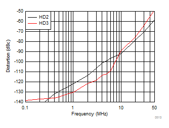
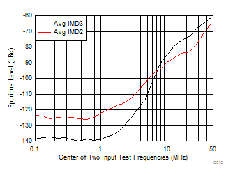
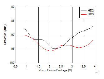
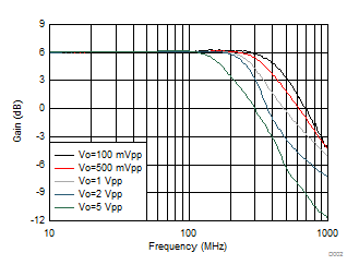
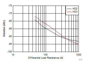
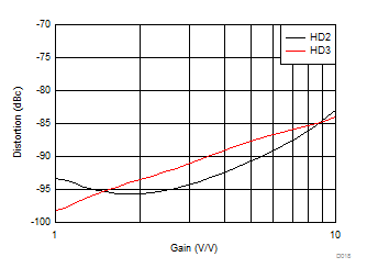
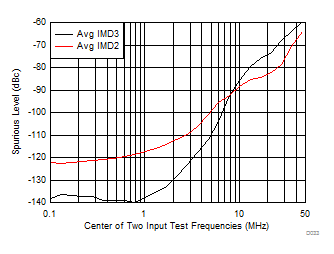
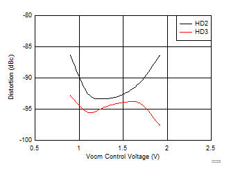
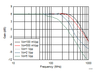
At Vs+ = 5 V, Vs– = GND, Vocm is open, 50-Ω single-ended input to differential output, gain = 2 V/V, Rload = 500 Ω, and TA ≈ 25°C (unless otherwise noted).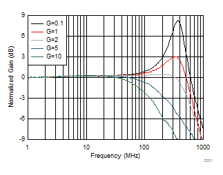 Figure 1. Small-Signal Frequency Response vs Gain
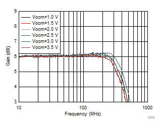
| Vout = 100 mVPP , see Figure 61 with Vocm adjusted |
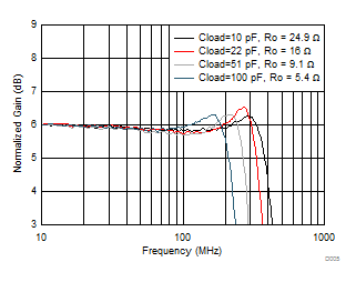
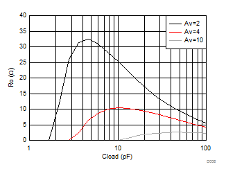
| 100 mVPP at load, Av = 2 (see Figure 71), two series Ro added at output before Cload |
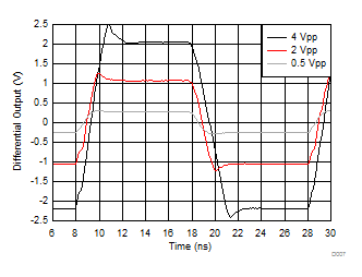
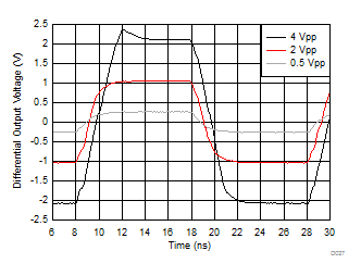
| 50-MHz input, 0.3-ns input edge rate, single-ended to differential output, DC coupled, see Figure 63 |
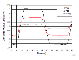
| G = 5 V/V, 50-MHz input, 0.3-ns input edge rate, single-ended input to differential output, see Figure 63 |
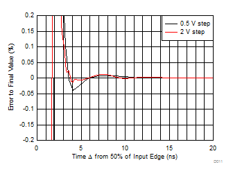
| Simulated with 2-ns input transition time, see Figure 63 | ||
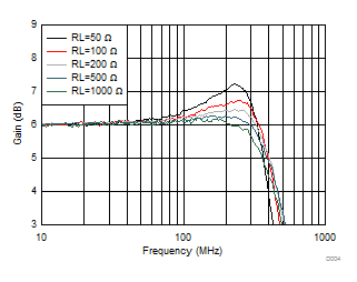
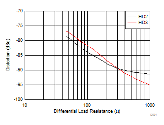
| Vout = 100 mVPP, see Figure 61 with RL adjusted |
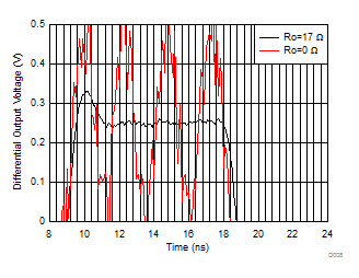
| Av = 2 , 500-mVPP output into 22-pF Cload, see Figure 71 | ||
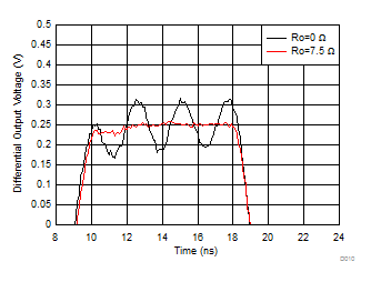 Figure 10. Step Response into Capacitive Load
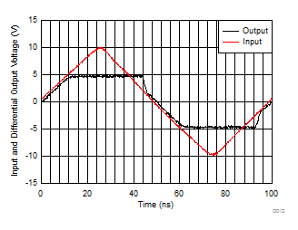
| Single-ended to differential gain of 2 (see Figure 63), 2x input overdrive |
7.7.2 3-V Single Supply
At Vs+ = 3 V, Vs– = GND, Vocm is open, 50-Ω single-ended input to differential output, gain = 2 V/V, Rload = 500 Ω, and TA ≈ 25°C (unless otherwise noted).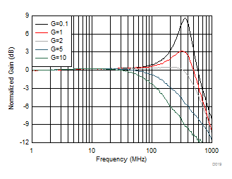 Figure 19. Small-Signal Frequency Response vs Gain
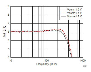
| Vout = 100 mVPP, see Figure 61 with Vocm adjusted |
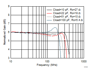
| 100 mVPP at load, Av = 2 (see Figure 71), two series Ro added at output before Cload |
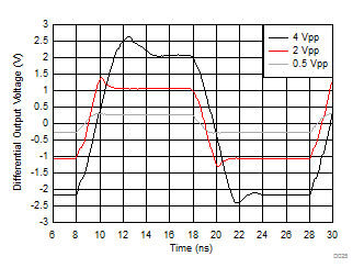
| 50-MHz input, 0.3-ns input edge rate, single-ended input to differential output, DC coupled, see Figure 63 |
| G = 5 V/V, 50-MHz input, 0.3-ns input edge rate, single-ended input to differential output, see Figure 61 |
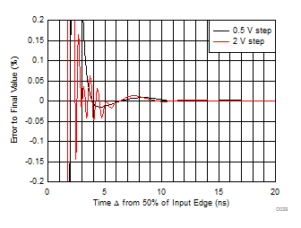
| Simulated with 2-ns input transition time, see Figure 63 | ||
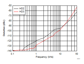
| 2-VPP output, see Figure 61 with Vs+ = 3 V, Vocm = 1.5 V |
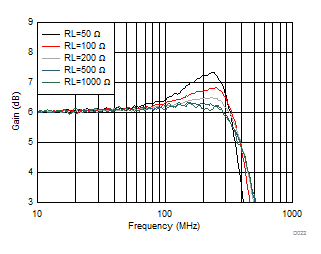
| Vout = 100 mVPP, see Figure 61 with the Rload adjusted |
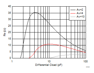 Figure 24. Recommended Ro vs Cload
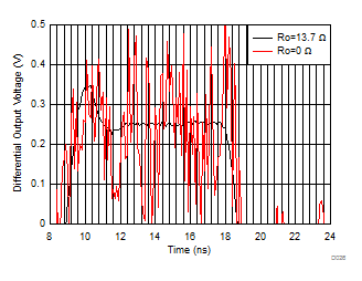
| 500-mVPP output into 22-pF Cload, see Figure 71 with Vs+ = 3 V and Vocm = 1.5 V |
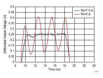 Figure 28. Step Response into Capacitive Load
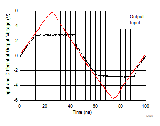
| Single-ended to differential gain of 2 (see Figure 63), > 2x input overdrive |
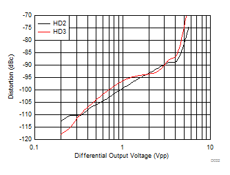
| f = 10 MHz, see Figure 61 with Vs+ = 3 V, Vocm = 1.5 V |
7.7.3 3-V to 5-V Supply Range
At Vs+ = 3 V and 5 V, Vs– = GND, Vocm is open, 50-Ω single-ended input to differential output, gain = 2 V/V, Rload = 500 Ω, and TA ≈ 25°C (unless otherwise noted).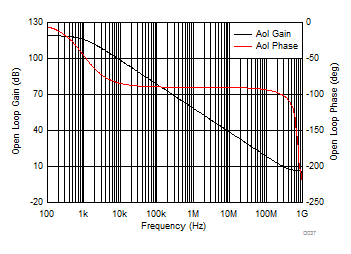
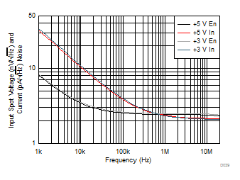
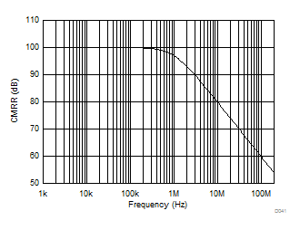
| Common-mode in to differential out, gain of 2 simulation | ||
 Figure 43. Common-Mode, Small- and Large-Signal Response (Vocm pin driven)
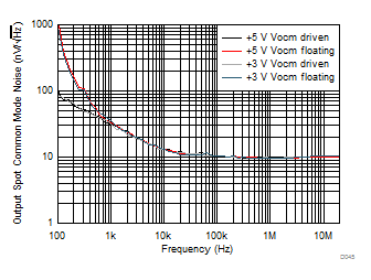
| Vocm input either driven to midsupply by low impedance source, or allowed to float and default to midsupply |
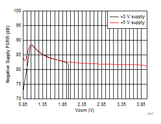
| Single-ended to differential gain of 2 (see Figure 61), PSRR for negative supply to differential output (1-kHz simulation) |
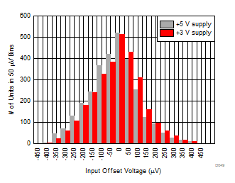
| 3 lots, total of 2962 units trimmed at 5-V supply |
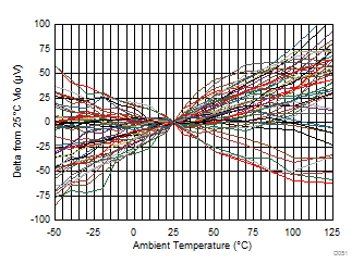
| 5-V and 3-V delta from 25°C VIO, 25 units |
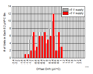
| –40°C to +125°C endpoint drift, 3 lots, total of 68 units |
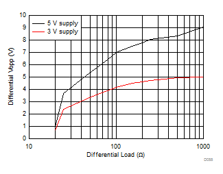
| Maximum differential output swing, Vocm at midsupply |
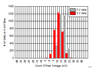
| Vocm input floating, 3 lots, total of 2962 units |
Default Value
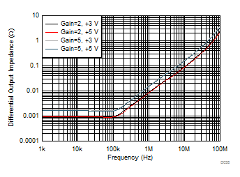
| Single-ended input to differential output, simulated differential output impedance, (closed-loop) gain of 2 and 5, see Figure 61 |
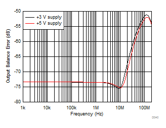
| Single-ended input to differential output, gain of 2 (see Figure 61), simulated with 1% resistor, worst-case mismatch |
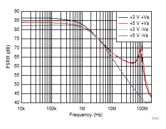
| Single-ended to differential, gain of 2 (see Figure 61) PSRR simulated to differential output |
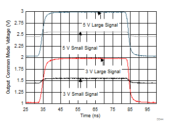 Figure 44. Common-Mode, Small- and Large-Step Response (Vocm pin driven)
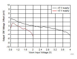
| Average Vocm output offset of 37 units, Standard deviation < 2.5 mV, see Figure 63 |
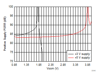
| Single-ended to differential gain of 2 (see Figure 61), PSRR for positive supply to differential output (1-kHz simulation) |
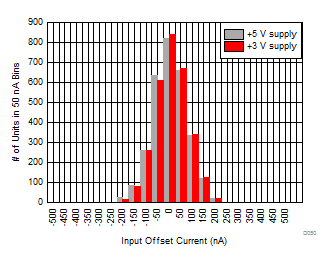
| 3 lots, total of 2962 units |
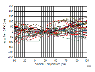
| 5-V and 3-V over temperature IOS, 25 units |
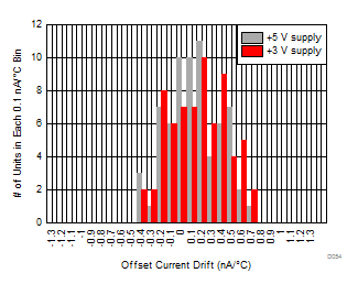
| –40°C to +125°C endpoint drift, 3 lots, total of 68 units |
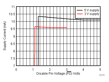
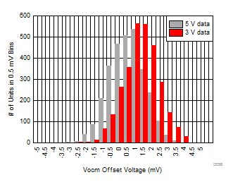
| Input driven midsupply, 3 lots, total of 2962 units |
