ZHCSEK0A November 2015 – November 2015 THS4541-Q1
PRODUCTION DATA.
- 1 特性
- 2 应用
- 3 说明
- 4 修订历史记录
- 5 Device Family Comparison
- 6 Pin Configuration and Functions
- 7 Specifications
-
8 Parameter Measurement Information
- 8.1 Example Characterization Circuits
- 8.2 Frequency-Response Shape Factors
- 8.3 I/O Headroom Considerations
- 8.4 Output DC Error and Drift Calculations and the Effect of Resistor Imbalances
- 8.5 Noise Analysis
- 8.6 Factors Influencing Harmonic Distortion
- 8.7 Driving Capacitive Loads
- 8.8 Thermal Analysis
-
9 Detailed Description
- 9.1 Overview
- 9.2 Functional Block Diagram
- 9.3 Feature Description
- 9.4
Device Functional Modes
- 9.4.1
Operation from Single-Ended Sources to Differential Outputs
- 9.4.1.1 AC-Coupled Signal Path Considerations for Single-Ended Input to Differential Output Conversion
- 9.4.1.2 DC-Coupled Input Signal Path Considerations for Single-Ended to Differential Conversion
- 9.4.1.3 Resistor Design Equations for the Single-Ended to Differential Configuration of the FDA
- 9.4.1.4 Input Impedance for the Single-Ended to Differential FDA Configuration
- 9.4.2 Differential-Input to Differential-Output Operation
- 9.4.1
Operation from Single-Ended Sources to Differential Outputs
- 10Application and Implementation
- 11Power-Supply Recommendations
- 12Layout
- 13器件和文档支持
- 14机械、封装和可订购信息
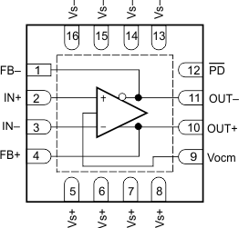
6 Pin Configuration and Functions
RGT Package
16-Pin VQFN With Exposed Thermal Pad
Top View

Pin Functions
| PIN | I/O | DESCRIPTION | |
|---|---|---|---|
| NAME | NO.(1) | ||
| FB+ | 4 | O | Noninverted (positive) output feedback |
| FB– | 1 | O | Inverted (negative) output feedback |
| IN+ | 2 | I | Noninverting (positive) amplifier input |
| IN– | 3 | I | Inverting (negative) amplifier input |
| NC | — | — | No internal connection |
| OUT+ | 10 | O | Noninverted (positive) amplifier output |
| OUT– | 11 | O | Inverted (negative) amplifier output |
| PD | 12 | I | Power down. PD = logic low = power off mode; PD = logic high = normal operation. |
| Vocm | 9 | I | Common-mode voltage input |
| Vs+ | 5 | I | Positive power-supply input |
| 6 | |||
| 7 | |||
| 8 | |||
| Vs– | 13 | I | Negative power-supply input |
| 14 | |||
| 15 | |||
| 16 | |||
(1) Solder the exposed thermal pad to a heat-spreading power or ground plane. This pad is electrically isolated from the die, but must be connected to a power or ground plane and not floated.