ZHCSEK0A November 2015 – November 2015 THS4541-Q1
PRODUCTION DATA.
- 1 特性
- 2 应用
- 3 说明
- 4 修订历史记录
- 5 Device Family Comparison
- 6 Pin Configuration and Functions
- 7 Specifications
-
8 Parameter Measurement Information
- 8.1 Example Characterization Circuits
- 8.2 Frequency-Response Shape Factors
- 8.3 I/O Headroom Considerations
- 8.4 Output DC Error and Drift Calculations and the Effect of Resistor Imbalances
- 8.5 Noise Analysis
- 8.6 Factors Influencing Harmonic Distortion
- 8.7 Driving Capacitive Loads
- 8.8 Thermal Analysis
-
9 Detailed Description
- 9.1 Overview
- 9.2 Functional Block Diagram
- 9.3 Feature Description
- 9.4
Device Functional Modes
- 9.4.1
Operation from Single-Ended Sources to Differential Outputs
- 9.4.1.1 AC-Coupled Signal Path Considerations for Single-Ended Input to Differential Output Conversion
- 9.4.1.2 DC-Coupled Input Signal Path Considerations for Single-Ended to Differential Conversion
- 9.4.1.3 Resistor Design Equations for the Single-Ended to Differential Configuration of the FDA
- 9.4.1.4 Input Impedance for the Single-Ended to Differential FDA Configuration
- 9.4.2 Differential-Input to Differential-Output Operation
- 9.4.1
Operation from Single-Ended Sources to Differential Outputs
- 10Application and Implementation
- 11Power-Supply Recommendations
- 12Layout
- 13器件和文档支持
- 14机械、封装和可订购信息
12 Layout
12.1 Layout Guidelines
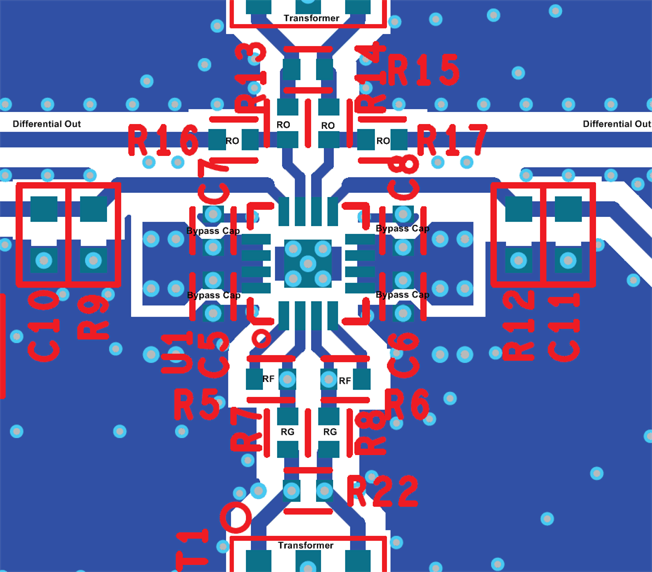
Similar to all high-speed devices, best system performance is achieved with a close attention to board layout. The THS4541-Q1 evaluation module (EVM) shows a good example of high frequency layout techniques as a reference. This EVM includes numerous extra elements and features for characterization purposes that may not apply to some applications. General high-speed, signal-path layout suggestions include:
- Continuous ground planes are preferred for signal routing with matched impedance traces for longer runs; however, open up both ground and power planes around the capacitive sensitive input and output device pins. After the signal is sent into a resistor, parasitic capacitance becomes more of a bandlimiting issue and less of a stability issue.
- Use good, high-frequency decoupling capacitors (0.1 µF) on the ground plane at the device power pins. Higher value capacitors (2.2 µF) are required, but may be placed further from the device power pins and shared among devices. For best high-frequency decoupling, consider X2Y supply-decoupling capacitors that offer a much higher self-resonance frequency over standard capacitors.
- When using differential signal routing over any appreciable distance, use microstrip layout techniques with matched impedance traces.
- Higher-speed FDAs, such as the THS4541-Q1, include a duplicate of the output pins on the input feedback side of the package. This duplication is intended to allow the external feedback resistors to be connected with virtually no trace length on the input side of the package. Use this layout approach with no extra trace length on this critical feedback path.
- The input summing junctions are very sensitive to parasitic capacitance. Connect any Rg elements into the summing junction with minimal trace length to the device pin side of the resistor. The other side of the Rg elements can have more trace length if needed to the source or to ground.
12.2 Layout Example
 Figure 82. Layout Example