ZHCSEK0A November 2015 – November 2015 THS4541-Q1
PRODUCTION DATA.
- 1 特性
- 2 应用
- 3 说明
- 4 修订历史记录
- 5 Device Family Comparison
- 6 Pin Configuration and Functions
- 7 Specifications
-
8 Parameter Measurement Information
- 8.1 Example Characterization Circuits
- 8.2 Frequency-Response Shape Factors
- 8.3 I/O Headroom Considerations
- 8.4 Output DC Error and Drift Calculations and the Effect of Resistor Imbalances
- 8.5 Noise Analysis
- 8.6 Factors Influencing Harmonic Distortion
- 8.7 Driving Capacitive Loads
- 8.8 Thermal Analysis
-
9 Detailed Description
- 9.1 Overview
- 9.2 Functional Block Diagram
- 9.3 Feature Description
- 9.4
Device Functional Modes
- 9.4.1
Operation from Single-Ended Sources to Differential Outputs
- 9.4.1.1 AC-Coupled Signal Path Considerations for Single-Ended Input to Differential Output Conversion
- 9.4.1.2 DC-Coupled Input Signal Path Considerations for Single-Ended to Differential Conversion
- 9.4.1.3 Resistor Design Equations for the Single-Ended to Differential Configuration of the FDA
- 9.4.1.4 Input Impedance for the Single-Ended to Differential FDA Configuration
- 9.4.2 Differential-Input to Differential-Output Operation
- 9.4.1
Operation from Single-Ended Sources to Differential Outputs
- 10Application and Implementation
- 11Power-Supply Recommendations
- 12Layout
- 13器件和文档支持
- 14机械、封装和可订购信息
10 Application and Implementation
NOTE
Information in the following applications sections is not part of the TI component specification, and TI does not warrant its accuracy or completeness. TI’s customers are responsible for determining suitability of components for their purposes. Customers should validate and test their design implementation to confirm system functionality.
10.1 Application Information
The THS4541-Q1 offers an effective solution over a broad range of applications. Two examples are developed here. First, an attenuator stage that directly receives a higher input signal voltage and translates it to a lower differential swing on a fixed common-mode is shown. This design requires some attention to frequency-response flatness issues, and one approach to managing these issues is shown. The second example is a gain of 2 V/V, matched input of 50 Ω to an output set to 0.95 V common-mode followed by a third-order Bessel filter with approximately 20 MHz of bandwidth feeding into the ADC34J22, a low-power, 12-bit, quad 50-MSPS JESD 204B ADC.
10.2 Typical Applications
10.2.1 Designing Attenuators
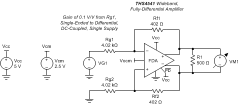 Figure 77. Divide-by-10 Attenuator Application for the THS4541-Q1
10.2.1.1 Design Requirements
In this design, the aim is to:
- Present a 4-kΩ input impedance to a ±40-V input signal (maximum ±10 mA from the prior stage).
- Attenuate that swing by a factor 1/10 (–20 dB) to a differential output swing.
- Place that swing on a 2.5-V common-mode voltage at the THS4541-Q1 outputs.
- Operate on a single +5-V supply and ground.
- Tune the frequency response to a flat Butterworth response with external capacitors.
10.2.1.2 Detailed Design Procedure
Operating the THS4541-Q1 at a low DC noise gain, or with higher feedback resistors, can cause a lower phase margin to exist, giving the response peaking shown in Figure 1 for the gain of 0.1 (a 1/10 attenuator) condition. Although it is often useful operating the THS4541-Q1 as an attenuator (taking a large input range to a purely differential signal around a controlled-output, common-mode voltage), the response peaking illustrated in Figure 1 is usually undesirable. Several methods can be used to reduce or eliminate this peaking; usually, at the cost of higher output noise. Using DC techniques always increases the output noise broadband, while using an ac noise-gain-shaping technique peaks the noise, but only at higher frequencies that can then be filtered off with the typical passive filters often used after this stage. Figure 77 shows a simplified schematic for the gain of 0.1 V/V test from Figure 61.
This configuration shows a nominal 18° phase margin (from Table 2); therefore, a very highly-peaked response is illustrated in Figure 1. This peaking can be eliminated by placing two feedback capacitors across the Rf elements and a differential input capacitor. Adding these capacitors provides a transition from a resistively set noise gain (NG1 here; 1.1 in Table 2) to a capacitive divider at high-frequency flattening out to a higher noise gain (NG2 here). The key for this approach is to target a Zo, where the noise gain begins to peak up. Using only the following terms, and targeting a closed-loop flat (Butterworth) response, gives this solution sequence for Zo and then the capacitor values.
- Gain bandwidth product in Hz (850 MHz for the THS4541-Q1)
- Low frequency noise gain, NG1 ( = 1.1 in the attenuator gain of 0.1 V/V design)
- Target high-frequency noise gain selected to be higher than NG1 (NG2 = 3.1 V/V is selected for this design)
- Feedback resistor value, Rf (assumed balanced for this differential design = 402 Ω for this design example)
From these elements, for any decompensated voltage-feedback op amp or FDA, solve for Zo (in Hz) using Equation 15:

From this target zero frequency in the noise gain, solve for the feedback capacitors using Equation 16:

The next step is to resolve the input capacitance on the summing junction. Equation 17 is for a single-ended op amp (for example, OPA847) where that capacitor goes to ground. To use Equation 17 for a voltage-feedback FDA, cut the target value in half, and place the result across the two inputs (reducing the external value by the specified internal differential capacitance).

Setting the external compensation elements using Equation 15 to Equation 17 allows an estimate of the resulting flat bandwidth f–3dB frequency, as shown in Equation 18:

Running through these steps for the THS4541-Q1 in the attenuator circuit of Figure 77 gives the proposed compensation of Figure 78 where Equation 18 estimates a bandwidth of 252 MHz (Zo target is 74.7 MHz).
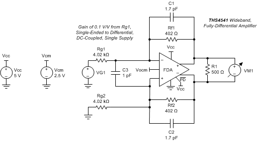 Figure 78. Compensated Attenuator Circuit Using the THS4541-Q1
The 1 pF across the inputs is really a total 1.85 pF, including the internal differential capacitance, and a Cs =
3.7 pF for a single-ended design from Equation 17.
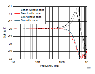
These two designs (with and without the capacitors) were both bench tested and simulated using the THS4541 TINA model giving the results of Figure 79.
This method does a good job of flattening the response for what starts out as a low phase-margin attenuator application. The simulation model does a very good job of predicting the peaking and showing the same improvement with the external capacitors; both giving a flat, approximately 250-MHz, closed-loop bandwidth for this gain of a 0.1-V/V design. In this example, the output noise begins to peak up (as a result of the noise-gain shaping of the capacitors) above 70 MHz. Use postfiltering to minimize any increase in the integrated noise using this technique. Using this solution to deliver an 8-VPP differential output to a successive approximation register (SAR) ADC (using the 2.5-V Vocm shown), the circuit accepts up to ±40-V inputs, where the 4-kΩ input Rg1 draws ±10 mA from the source.
10.2.1.3 Application Curve
10.2.2 Interfacing to High-Performance ADCs
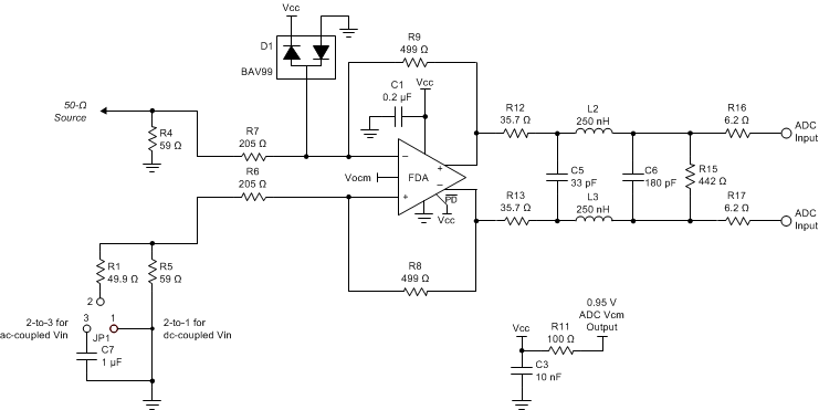 Figure 80. DC-Coupled, Bipolar Input Gain of 2 V/V Single-Ended to Differential Interface to ADC
10.2.2.1 Design Requirements
In this example design, an impedance matched input assuming a 50-Ω source is implemented with a DC-coupled gain of 2 V/V to the ADC. This configuration effectively reduces the required full-scale input to ±0.5 V for a 2-VPP full-scale input ADC. Add a low insertion-loss interstage filter to the ADC to control the broadband noise where the goal is to show minimal SNR reduction in the FFT, as well as minimal degradation in SFDR performance.
10.2.2.2 Detailed Design Procedure
The THS4541-Q1 provides a very flexible element for interfacing from a variety of sources to a wide range of ADCs. Because all precision and high-speed ADCs require a differential input on a common-mode voltage, this design is the primary application for the THS4541-Q1.
The THS4541-Q1 provides a simple interface to a wide variety of precision SAR, ΔΣ, or higher-speed pipeline ADCs. To deliver the exceptional distortion at the output pins, considerably wider bandwidth than typically required in the signal path to the ADC inputs is provided by the THS4541-Q1. For instance, the gain of 2 single-ended to differential design example provides approximately a 500-MHz, small-signal bandwidth. Even if the source signal is Nyquist bandlimited, this broad bandwidth can possibly integrate enough THS4541-Q1 noise to degrade the SNR through the ADC if the broadband noise is not bandlimited between the amplifier and ADC.
Figure 80 shows an example DC-coupled, gain of 2 interface with a controlled, interstage-bandwidth filter implemented on the demonstration board for the JESD digital-output interface, ADC34J22 (a 50-MSPS, quad, 12-bit ADC). This board is called the DEV-ADC34J22 ADC HSMC MODULE with complete documentation at http://dallaslogic.com/prod_dev-adc34j/.
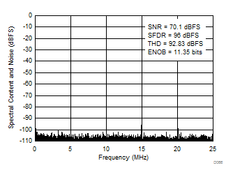
Designed for a DC-coupled 50Ω input match, this design starts with a 499-Ω feedback resistor, and provides a gain of 2.35V/V to the THS4541-Q1 output pins. The third-order interstage, low-pass filter provides a 20-MHz Bessel response with a 0.85 V/V insertion loss to the ADC, providing a net gain of 2 V/V from board edge to the ADC inputs. Although the THS4541-Q1 can absorb overdrives, an external protection element is added using the BAV99 low-capacitance device, shown in Figure 80. For DC-coupled testing, pins 1 and 2 are jumpered together. When the source is an AC-coupled, 50-Ω source, pins 2 and 3 are jumpered to maintain differential balance. FFT testing normally uses a bandpass filter into the board; an AC-coupled source. A typical 5-MHz, full-scale, single-tone FFT is shown in Figure 81, where the jumper is placed from pins 2 to 3. The reported SNR of 70.09 dBFs is only a slight reduction from the tested ADC-only performance of 70.42 dBFs, showing the value of the interstage noise bandwidth limiting filter. The exceptionally low harmonic distortion for the THS4541-Q1 also shows up in the very low SFDR and THD shown in Figure 81. This 96-dB SFDR and 92.83-dB THD are comparable to the ADC-only test results.
