SN65LVDS33-EP
- Controlled Baseline — One Assembly/Test Site, One Fabrication Site
- Extended Temperature Performance of Up to -55°C to 125°C
- Enhanced Diminishing Manufacturing Sources (DMS) Support
- Enhanced Product-Change Notification
- Qualification Pedigree(1)
- 400-Mbps Signaling Rate(2) and 200-Mxfr/s Data Transfer Rate
- Operates With a Single 3.3-V Supply
- -4-V to 5-V Common-Mode Input Voltage Range
- Differential Input Thresholds < ±50 mV With 50 mV of Hysteresis Over Entire Common-Mode Input Voltage Range
- Integrated 110-
 Line Termination Resistors On LVDT Products
 - Complies With TIA/EIA-644 (LVDS)
- Active Failsafe Assures a High-Level Output With No Input
- Bus-Pin ESD Protection Exceeds 15-kV HBM
- Input Remains High-Impedance On Power Down
- TTL Inputs Are 5-V Tolerant
- Pin-Compatible With the AM26LS32, SN65LVDS32B, µA9637, SN65LVDS9637B
(1) Component qualification in accordance with JEDEC and industry standards to ensure reliable operation over an extended temperature range. This includes, but is not limited to, Highly Accelerated Stress Test (HAST) or biased 85/85, temperature cycle, autoclave or unbiased HAST, electromigration, bond intermetallic life, and mold compound life. Such qualification testing should not be viewed as justifying use of this component beyond specified performance and environmental limits.
(2) The signaling rate of a line is the number of voltage transitions that are made per second expressed in the units bps (bits per second).
This family of four LVDS data line receivers offers the widest common-mode input voltage range in the industry. These receivers provide an input voltage range specification compatible with a 5-V PECL signal as well as an overall increased ground-noise tolerance. They are in industry standard footprints with integrated termination as an option.
Precise control of the differential input voltage thresholds allows for inclusion of 50 mV of input voltage hysteresis to improve noise rejection on slowly changing input signals. The input thresholds are still no more than +50 mV over the full input common-mode voltage range.
The high-speed switching of LVDS signals usually necessitates the use of a line impedance matching resistor at the receiving-end of the cable or transmission media. The SN65LVDT series of receivers eliminates this external resistor by integrating it with the receiver. The nonterminated SN65LVDS series is also available for multidrop or other termination circuits.
The receivers can withstand ±15-kV human-body model (HBM) and ±600-V machine model (MM) electrostatic discharges to the receiver input pins with respect to ground without damage. This provides reliability in cabled and other connections where potentially damaging noise is always a threat.
The receivers also include a (patent pending) failsafe circuit that provides a high-level output within 600 ns after loss of the input signal. The most common causes of signal loss are disconnected cables, shorted lines, or powered-down transmitters. The failsafe circuit prevents noise from being received as valid data under these fault conditions. This feature may also be used for Wired-Or bus signaling. See The Active Failsafe Feature of the SN65LVDS32B application note.
The intended application and signaling technique of these devices is point-to-point baseband data transmission over controlled impedance media of approximately 100 . The transmission media may be printed-circuit board traces, backplanes, or cables. The ultimate rate and distance of data transfer is dependent upon the attenuation characteristics of the media and the noise coupling to the environment.
The SN65LVDS33-EP is characterized for operation from -55°C to 125°C.
技术文档
| 类型 | 标题 | 下载最新的英语版本 | 日期 | |||
|---|---|---|---|---|---|---|
| * | 数据表 | SN65LVDS33-EP High-Speed Differential Receivers 数据表 (Rev. B) | 2007年 4月 19日 | |||
| * | VID | SN65LVDS33-EP VID V6205614 | 2016年 6月 21日 | |||
| * | 辐射与可靠性报告 | SN65LVDS33MDREP Reliability Report | 2013年 9月 6日 | |||
| 应用简报 | LVDS to Improve EMC in Motor Drives | 2018年 9月 27日 | ||||
| 应用简报 | How Far, How Fast Can You Operate LVDS Drivers and Receivers? | 2018年 8月 3日 | ||||
| 应用简报 | How to Terminate LVDS Connections with DC and AC Coupling | 2018年 5月 16日 |
设计和开发
如需其他信息或资源,请点击以下任一标题进入详情页面查看(如有)。
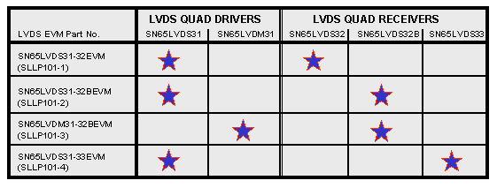
SN65LVDS31-33EVM — 用于 SN65LVDS31 和 SN65LVDS33 的评估模块
TI offers a series of low-voltage differential signaling (LVDS) evaluation modules (EVMs) designed for analysis of the electrical characteristics of LVDS drivers and receivers. Four unique EVMs are available to evaluate the different classes of LVDS devices offered by TI.
As seen in the Combination (...)
PSPICE-FOR-TI — 适用于 TI 设计和模拟工具的 PSpice®
借助 PSpice for TI 的设计和仿真环境及其内置的模型库,您可对复杂的混合信号设计进行仿真。创建完整的终端设备设计和原型解决方案,然后再进行布局和制造,可缩短产品上市时间并降低开发成本。
在 PSpice for TI 设计和仿真工具中,您可以搜索 TI (...)
TINA-TI — 基于 SPICE 的模拟仿真程序
TINA-TI 安装需要大约 500MB。直接安装,如果想卸载也很容易。我们相信您肯定会爱不释手。
TINA 是德州仪器 (TI) 专有的 DesignSoft 产品。该免费版本具有完整的功能,但不支持完整版 TINA 所提供的某些其他功能。
如需获取可用 TINA-TI 模型的完整列表,请参阅:SpiceRack - 完整列表
需要 HSpice (...)
| 封装 | 引脚 | 下载 |
|---|---|---|
| SOIC (D) | 16 | 查看选项 |
订购和质量
- RoHS
- REACH
- 器件标识
- 引脚镀层/焊球材料
- MSL 等级/回流焊峰值温度
- MTBF/时基故障估算
- 材料成分
- 鉴定摘要
- 持续可靠性监测
- 制造厂地点
- 封装厂地点
推荐产品可能包含与 TI 此产品相关的参数、评估模块或参考设计。