SLLS933G November 2008 – January 2015 SN65HVD233-HT
PRODUCTION DATA.
- 1 Features
- 2 Applications
- 3 Description
- 4 Revision History
- 5 Description (Continued)
- 6 Pin Configuration and Functions
-
7 Specifications
- 7.1 Absolute Maximum Ratings
- 7.2 ESD Ratings
- 7.3 Recommended Operating Conditions
- 7.4 Thermal Information
- 7.5 Driver Electrical Characteristics
- 7.6 Receiver Electrical Characteristics
- 7.7 Driver Switching Characteristics
- 7.8 Receiver Switching Characteristics
- 7.9 Device Switching Characteristics
- 7.10 Typical Characteristics
- 8 Parameter Measurement Information
- 9 Detailed Description
- 10Application and Implementation
- 11Power Supply Recommendations
- 12Layout
- 13Device and Documentation Support
- 14Mechanical, Packaging, and Orderable Information
封装选项
机械数据 (封装 | 引脚)
散热焊盘机械数据 (封装 | 引脚)
订购信息
7 Specifications
7.1 Absolute Maximum Ratings
over operating free-air temperature range (unless otherwise noted) (1)(2)| MIN | MAX | UNIT | ||
|---|---|---|---|---|
| VCC | Supply voltage range | –0.3 | 7 | V |
| Voltage range at any bus terminal (CANH or CANL) | –36 | 36 | V | |
| Voltage input range, transient pulse (CANH and CANL) through 100 Ω (see Figure 19) | –100 | 100 | V | |
| VI | Input voltage range (D, R, RS, LBK) | –0.5 | 7 | V |
| IO | Receiver output current | –10 | 10 | mA |
| Tstg | Storage temperature | –65 | 150 | °C |
(1) Stresses beyond those listed under Absolute Maximum Ratings may cause permanent damage to the device. These are stress ratings only, which do not imply functional operation of the device at these or any other conditions beyond those indicated under Recommended Operating Conditions. Exposure to absolute-maximum-rated conditions for extended periods may affect device reliability.
(2) All voltage values, except differential I/O bus voltages, are with respect to network ground terminal.
7.2 ESD Ratings
| VALUE | UNIT | |||||
|---|---|---|---|---|---|---|
| V(ESD) | Electrostatic discharge | Human body model (HBM), per ANSI/ESDA/JEDEC JS-001, all pins(1) | CANH, CANL, and GND | ±16000 | V | |
| All pins | ±3000 | |||||
| Charged device model (CDM), per JEDEC specification JESD22-C101, all pins(2) | ±1000 | |||||
(1) JEDEC document JEP155 states that 500-V HBM allows safe manufacturing with a standard ESD control process.
(2) JEDEC document JEP157 states that 250-V CDM allows safe manufacturing with a standard ESD control process.
7.3 Recommended Operating Conditions
TA = –55°C to 210°C| MIN | MAX | UNIT | |||
|---|---|---|---|---|---|
| VCC | Supply voltage | 3 | 3.6 | V | |
| Voltage at any bus terminal (separately or common mode) | –7 | 12 | V | ||
| VIH | High-level input voltage | D, LBK | 2 | 5.5 | V |
| VIL | Low-level input voltage | D, LBK | 0 | 0.8 | V |
| VID | Differential input voltage | –6 | 6 | V | |
| Resistance from RS to ground | 0 | 100 | kΩ | ||
| VI(Rs) | Input voltage at RS for standby | 0.75 VCC | 5.5 | V | |
| IOH | High-level output current | Driver | –50 | mA | |
| Receiver | –10 | ||||
| IOL | Low-level output current | Driver | 50 | mA | |
| Receiver | 10 | ||||
| TJ | Operating junction temperature | 212 | °C | ||
| TA | Operating free-air temperature(1) | –55 | 210 | °C | |
(1) Maximum free-air temperature operation is allowed as long as the device maximum junction temperature is not exceeded.
7.4 Thermal Information
| THERMAL METRIC(1) | SN65HVD233-HT | UNIT | |||
|---|---|---|---|---|---|
| D | HJK/HKQ | JDJ | |||
| 8 PINS | 8 PINS | 8 PINS | |||
| RθJA | Junction-to-ambient thermal resistance | 106.4 | 146.1 | 72.7 | °C/W |
| RθJC(top) | Junction-to-case (top) thermal resistance | 55.8 | 23.7 | 3.1 | |
| RθJB | Junction-to-board thermal resistance | 46.5 | 152.0 | 38.3 | |
| ψJT | Junction-to-top characterization parameter | 10.7 | 20.7 | 6.0 | |
| ψJB | Junction-to-board characterization parameter | 45.9 | 93.1 | 26.9 | |
(1) For more information about traditional and new thermal metrics, see the IC Package Thermal Metrics application report, SPRA953.
7.5 Driver Electrical Characteristics
over operating free-air temperature range (unless otherwise noted)| PARAMETER | TEST CONDITIONS | TA = –55°C to 125°C | TA = 175°C(1) | TA = 210°C(2) | UNIT | |||||||||
|---|---|---|---|---|---|---|---|---|---|---|---|---|---|---|
| MIN | TYP | MAX | MIN | TYP | MAX | MIN | TYP | MAX | ||||||
| VO(D) | Bus output voltage (dominant) |
CANH | D = 0 V, RS = 0 V, See Figure 13 and Figure 14 |
2.45 | VCC | 2.45 | VCC | 2.45 | VCC | V | ||||
| CANL | 0.5 | 1.25 | 0.5 | 1.25 | 0.5 | 1.25 | ||||||||
| VO | Bus output voltage (recessive) | CANH | D = 3 V, RS = 0 V, See Figure 13 and Figure 14 |
2.3 | 2.3 | 2.3 | V | |||||||
| CANL | 2.3 | 2.3 | 2.3 | |||||||||||
| VOD(D) | Differential output voltage (Dominant) | D = 0 V, RS = 0 V, See Figure 13 and Figure 14 |
1.5 | 2 | 3 | 1.4 | 1.75 | 3 | 1.4 | 1.75 | 3 | V | ||
| D = 0 V, RS = 0 V, See Figure 14 and Figure 15 |
1.1 | 2 | 3 | 1.1 | 1.47 | 3 | 1.1 | 1.47 | 3 | |||||
| VOD | Differential output voltage (Recessive) | D = 3 V, RS = 0 V, See Figure 13 and Figure 14 |
–120 | 12 | –120 | 12 | –120 | 12 | mV | |||||
| D = 3 V, RS = 0 V, No load | –0.5 | 0.05 | –0.5 | 0.8 | –0.5 | 1.2 | V | |||||||
| VOC(pp) | Peak-to-peak common-mode output voltage | See Figure 21 | 1 | 1 | 1 | V | ||||||||
| IIH | High-level input current | D, LBK | D = 2 V | –30 | 30 | –30 | 30 | –30 | 30 | μA | ||||
| IIL | Low-level input current | D, LBK | D = 0.8 V | –30 | 30 | –30 | 30 | –30 | 30 | μA | ||||
| IOS | Short-circuit output current | VCANH = –7 V, CANL open, See Figure 24 |
–250 | –250 | –250 | mA | ||||||||
| VCANH = 12 V, CANL open, See Figure 24 |
1 | 1 | 1 | |||||||||||
| VCANL = –7 V, CANH open, See Figure 24 |
–1 | –1 | –1 | |||||||||||
| VCANL = 12 V, CANH open, See Figure 24 |
250 | 250 | 250 | |||||||||||
| CO | Output capacitance | See receiver input capacitance | ||||||||||||
| IIRs(s) | RS input current for standby | RS = 0.75 VCC | –10 | –10 | –10 | μA | ||||||||
| ICC | Supply current | Standby | RS = VCC, D = VCC, LBK = 0 V |
200 | 600 | 400 | 600 | 400 | 600 | μA | ||||
| Dominant | D = 0 V, No load, LBK = 0 V, RS = 0 V |
6 | 6 | 6 | mA | |||||||||
| Recessive | D =t VCC, No load, LBK = 0 V, RS = 0 V |
6 | 6 | 6 | ||||||||||
(1) Minimum and maximum parameters are characterized for operation at TA = 175°C and production tested at TA = 125°C.
(2) Minimum and maximum parameters are characterized for operation at TA = 210°C but may not be production tested at that temperature. Production test limits with statistical guardbands are used to ensure high temperature performance.
7.6 Receiver Electrical Characteristics
over operating free-air temperature range (unless otherwise noted)| PARAMETER | TEST CONDITIONS | TA = –55°C to 125°C | TA = 175°C(1) | TA = 210°C(2) | UNIT | |||||||||
|---|---|---|---|---|---|---|---|---|---|---|---|---|---|---|
| MIN | TYP | MAX | MIN | TYP | MAX | MIN | TYP | MAX | ||||||
| VIT+ | Positive-going input threshold voltage | LBK = 0 V, See Table 1 | 620 | 900 | 600 | 900 | 600 | 900 | mV | |||||
| VIT– | Negative-going input threshold voltage | 500 | 715 | 500 | 725 | 500 | 725 | mV | ||||||
| Vhys | Hysteresis voltage (VIT+ – VIT–) |
100 | 140 | 140 | mV | |||||||||
| VOH | High-level output voltage | IO = –4 mA, See Figure 18 | 2.4 | 2.4 | 2.4 | V | ||||||||
| VOL | Low-level output voltage | IO = 4 mA, See Figure 18 | 0.4 | 0.4 | 0.4 | V | ||||||||
| II | Bus input current | CANH or CANL = 12 V |
Other bus pin = 0 V, D = 3 V, LBK = 0 V, RS = 0 V, |
140 | 500 | 140 | 500 | 140 | 500 | μA | ||||
| CANH or CANL = 12 V, VCC = 0 V |
200 | 600 | 200 | 700 | 200 | 800 | ||||||||
| CANH or CANL = –7 V |
–610 | –150 | –610 | –150 | –610 | –150 | ||||||||
| CANH or CANL = –7 V, VCC = 0 V |
–450 | –130 | –450 | –130 | –450 | –130 | ||||||||
| CI | Input capacitance (CANH or CANL) |
Pin to ground, VI = 0.4 sin (4E6πt) + 0.5 V, D = 3 V, LBK = 0 V |
45 | 55 | 55 | pF | ||||||||
| CID | Differential input capacitance | Pin to pin, VI = 0.4 sin (4E6πt) + 0.5 V, D = 3 V, LBK = 0 V |
15 | 15 | 15 | pF | ||||||||
| RID | Differential input resistance | D = 3 V, LBK = 0 V | 40 | 110 | 40 | 110 | 40 | 110 | kΩ | |||||
| RIN | Input resistance (CANH or CANL) |
20 | 51 | 19 | 51 | 18 | 51 | kΩ | ||||||
| ICC | Supply current | Standby | RS = VCC, D = VCC, LBK = 0 V | 200 | 600 | 400 | 600 | 400 | 600 | μA | ||||
| Dominant | D = 0 V, No load, RS = 0 V, LBK = 0 V |
6 | 6 | 6 | mA | |||||||||
| Recessive | D = VCC, No load, RS = 0 V, LBK = 0 V |
6 | 6 | 6 | ||||||||||
(1) Minimum and maximum parameters are characterized for operation at TA = 210°C and are not chacterized or production tested at
TA = 175°C.
TA = 175°C.
(2) Minimum and maximum parameters are characterized for operation at TA = 210°C but may not be production tested at that temperature. Production test limits with statistical guardbands are used to ensure high temperature performance.
7.7 Driver Switching Characteristics
over operating free-air temperature range (unless otherwise noted)| PARAMETER | TEST CONDITIONS | TA = –55°C to 125°C | TA = 175°C(1) | TA = 210°C(2) | UNIT | |||||||
|---|---|---|---|---|---|---|---|---|---|---|---|---|
| MIN | TYP | MAX | MIN | TYP | MAX | MIN | TYP | MAX | ||||
| tPLH | Propagation delay time, low-to-high-level output |
RS = 0 V, See Figure 16 | 35 | 85 | 50 | 50 | ns | |||||
| RS with 10 kΩ to ground, See Figure 16 |
70 | 125 | 75 | 75 | ||||||||
| RS with 100 kΩ to ground, See Figure 16 |
500 | 870 | 500 | 500 | ||||||||
| tPHL | Propagation delay time, high-to-low-level output |
RS = 0 V, See Figure 16 |
70 | 120 | 70 | 70 | ns | |||||
| RS with 10 kΩ to ground, See Figure 16 |
130 | 180 | 130 | 130 | ||||||||
| RS with 100 kΩ to ground, See Figure 16 |
870 | 1200 | 870 | 870 | ||||||||
| tsk(p) | Pulse skew (|tPHL – tPLH|) |
RS = 0 V, See Figure 16 |
35 | 9 | 9 | ns | ||||||
| RS with 10 kΩ to ground, See Figure 16 |
60 | 35 | 35 | |||||||||
| RS with 100 kΩ to ground, See Figure 16 |
370 | 475 | 475 | |||||||||
| tr | Differential output signal rise time | RS = 0 V, See Figure 16 | 20 | 70 | 20 | 75 | 20 | 75 | ns | |||
| tf | Differential output signal fall time | 18 | 70 | 20 | 75 | 20 | 75 | |||||
| tr | Differential output signal rise time | RS with 10 kΩ to ground, See Figure 16 |
30 | 135 | 30 | 140 | 30 | 140 | ns | |||
| tf | Differential output signal fall time | 30 | 135 | 30 | 140 | 30 | 140 | |||||
| tr | Differential output signal rise time | RS with 100 kΩ to ground, See Figure 16 |
250 | 1400 | 250 | 1400 | 250 | 1400 | ns | |||
| tf | Differential output signal fall time | 350 | 1400 | 350 | 1400 | 350 | 1400 | |||||
| ten(s) | Enable time from standby to dominant | See Figure 20 | 0.6 | 1.5 | 0.6 | 1.5 | 0.6 | 1.5 | μs | |||
(1) Minimum and maximum parameters are characterized for operation at TA = 210°C but not production tested at TA = 175°C or 210°C.
(2) Minimum and maximum parameters are characterized for operation at TA = 210°C but may not be production tested at that temperature. Production test limits with statistical guardbands are used to ensure high temperature performance.
7.8 Receiver Switching Characteristics
over operating free-air temperature range (unless otherwise noted)| PARAMETER | TEST CONDITIONS | TA = –55°C to 125°C | TA = 175°C(1) | TA = 210°C(2) | UNIT | |||||||
|---|---|---|---|---|---|---|---|---|---|---|---|---|
| MIN | TYP | MAX | MIN | TYP | MAX | MIN | TYP | MAX | ||||
| tPLH | Propagation delay time, low-to-high-level output | See Figure 18 | 35 | 60 | 50 | 60 | 50 | 60 | ns | |||
| tPHL | Propagation delay time, high-to-low-level output | 35 | 60 | 45 | 60 | 45 | 60 | ns | ||||
| tsk(p) | Pulse skew (|tPHL – tPLH|) | 7 | 5 | 5 | ns | |||||||
| tr | Output signal rise time | 2 | 6.5 | 6.5 | 8 | 6.5 | 8 | ns | ||||
| tf | Output signal fall time | 2 | 6.5 | 6.5 | 9 | 6.5 | 9 | ns | ||||
(1) Minimum and maximum parameters are characterized for operation at TA = 210°C but not production tested at TA = 175°C or 210°C.
(2) Minimum and maximum parameters are characterized for operation at TA = 210°C but may not be production tested at that temperature. Production test limits with statistical guardbands are used to ensure high temperature performance.
7.9 Device Switching Characteristics
over operating free-air temperature range (unless otherwise noted)| PARAMETER | TEST CONDITIONS | TA = –55°C to 125°C | TA = 175°C(1) | TA = 210°C(2) | UNIT | ||||||||
|---|---|---|---|---|---|---|---|---|---|---|---|---|---|
| MIN | TYP | MAX | MIN | TYP | MAX | MIN | TYP | MAX | |||||
| t(LBK) | Loopback delay, driver input to receiver output | See Figure 23 | 7.5 | 15 | 12 | 15 | 12 | 15 | ns | ||||
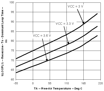
| t(loop1) | Total loop delay, driver input to receiver output, recessive to dominant | RS = 0 V, See Figure 22 | 70 | 135 | 90 | 135 | 90 | 135 | ns | ||||
| RS with 10 kΩ to ground, See Figure 22 |
105 | 190 | 115 | 190 | 115 | 190 | |||||||
| RS with 100 kΩ to ground, See Figure 22 |
535 | 1000 | 430 | 1000 | 430 | 1000 | |||||||
| t(loop2) | Total loop delay, driver input to receiver output, dominant to recessive | RS = 0 V, See Figure 22 | 70 | 135 | 98 | 135 | 98 | 135 | ns | ||||
| RS with 10 kΩ to ground, See Figure 22 |
105 | 190 | 150 | 190 | 150 | 190 | |||||||
| RS with 100 kΩ to ground, See Figure 22 |
535 | 1100 | 880 | 1200 | 880 | 1200 | |||||||
(1) Minimum and maximum parameters are characterized for operation at TA = 210°C but not production tested at TA = 175°C or 210°C.
(2) Minimum and maximum parameters are characterized for operation at TA = 210°C but may not be production tested at that temperature. Production test limits with statistical guardbands are used to ensure high temperature performance.
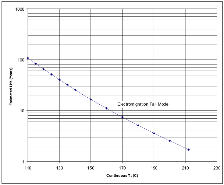
A. See the Specificationsfor absolute maximum and minimum recommended operating conditions.
B. Silicon operating life design goal is 10 years at 105°C junction temperature (does not include package interconnect life).
Figure 1. Operating Life Derating ChartSN65HVD233HD, SN65HVD233SJD, SN65HVD233SKGDA, SN65HVD233SHKJ, SN65HVD233SHKQ
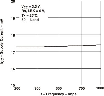
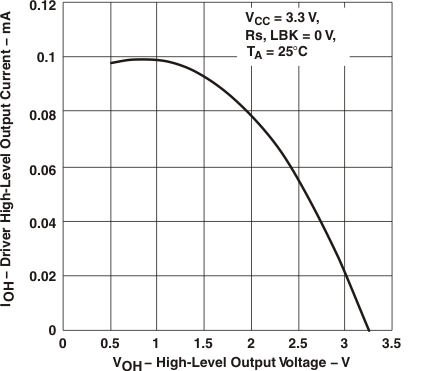
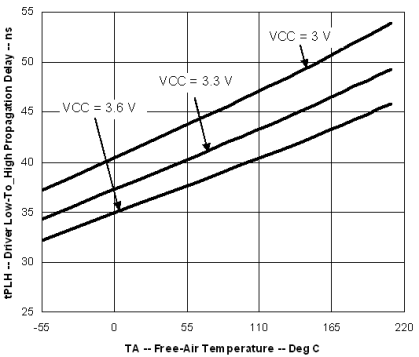
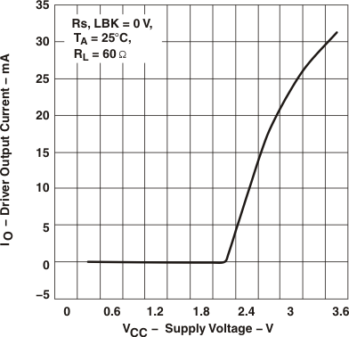
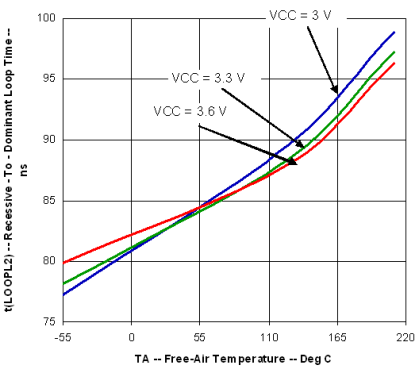
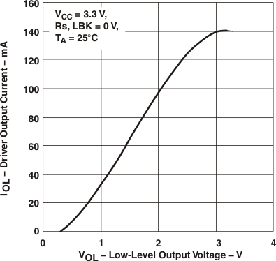
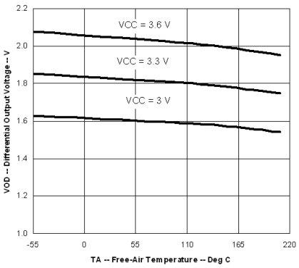
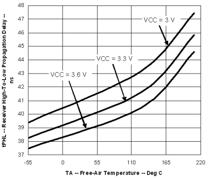
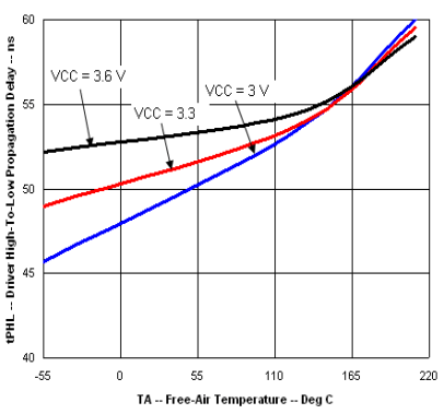
7.10 Typical Characteristics
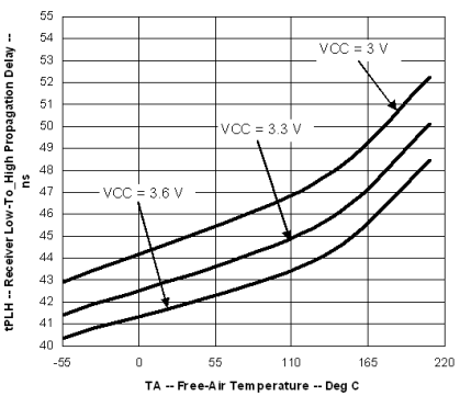
vs Free-Air Temperature
vs Free-Air Temperature