SLLS933G November 2008 – January 2015 SN65HVD233-HT
PRODUCTION DATA.
- 1 Features
- 2 Applications
- 3 Description
- 4 Revision History
- 5 Description (Continued)
- 6 Pin Configuration and Functions
-
7 Specifications
- 7.1 Absolute Maximum Ratings
- 7.2 ESD Ratings
- 7.3 Recommended Operating Conditions
- 7.4 Thermal Information
- 7.5 Driver Electrical Characteristics
- 7.6 Receiver Electrical Characteristics
- 7.7 Driver Switching Characteristics
- 7.8 Receiver Switching Characteristics
- 7.9 Device Switching Characteristics
- 7.10 Typical Characteristics
- 8 Parameter Measurement Information
- 9 Detailed Description
- 10Application and Implementation
- 11Power Supply Recommendations
- 12Layout
- 13Device and Documentation Support
- 14Mechanical, Packaging, and Orderable Information
封装选项
机械数据 (封装 | 引脚)
散热焊盘机械数据 (封装 | 引脚)
订购信息
8 Parameter Measurement Information
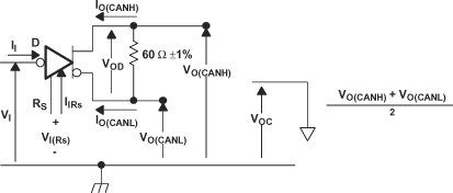 Figure 13. Driver Voltage, Current, and Test Definition
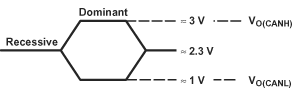 Figure 14. Bus Logic State Voltage Definitions
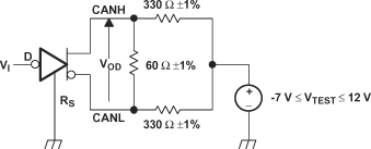 Figure 15. Driver VOD
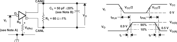
A. The input pulse is supplied by a generator having the following characteristics: Pulse repetition rate (PRR) ≤ 125 kHz, 50% duty cycle, tr ≤ 6 ns, tf ≤ 6 ns, ZO = 50 Ω.
B. CL includes fixture and instrumentation capacitance.
Figure 16. Driver Test Circuit and Voltage Waveforms
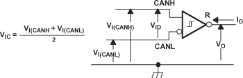 Figure 17. Receiver Voltage and Current Definitions
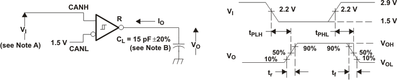
A. The input pulse is supplied by a generator having the following characteristics: Pulse repetition rate (PRR) ≤ 125 kHz, 50% duty cycle, tr ≤ 6 ns, tf ≤ 6 ns, ZO = 50 Ω.
B. CL includes fixture and instrumentation capacitance.
Figure 18. Receiver Test Circuit and Voltage Waveforms
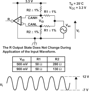
Table 1. Differential Input Voltage Threshold Test
| INPUT | OUTPUT | MEASURED | ||
|---|---|---|---|---|
| VCANH | VCANL | R | |VID| | |
| –6.1 V | –7 V | L | VOL | 900 mV |
| 12 V | 11.1 V | L | 900 mV | |
| –1 V | –7 V | L | 6 V | |
| 12 V | 6 V | L | 6 V | |
| –6.5 V | –7 V | H | VOH | 500 mV |
| 12 V | 11.5 V | H | 500 mV | |
| –7 V | –1 V | H | 6 V | |
| 6 V | 12 V | H | 6 V | |
| Open | Open | H | X | |
This test is conducted to test survivability only. Data stability at the R output is not specified.
Figure 19. Test Circuit, Transient Overvoltage Test
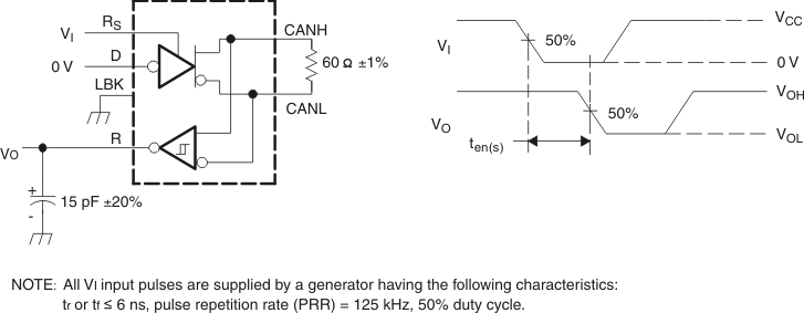 Figure 20. Ten(s) Test Circuit and Voltage Waveforms
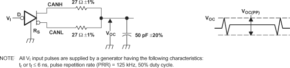 Figure 21. VOC(pp) Test Circuit and Voltage Waveforms
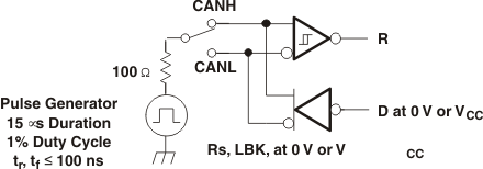
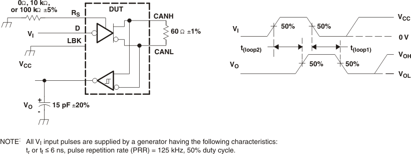 Figure 22. T(loop) Test Circuit and Voltage Waveforms
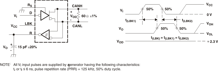 Figure 23. T(LBK) Test Circuit and Voltage Waveforms
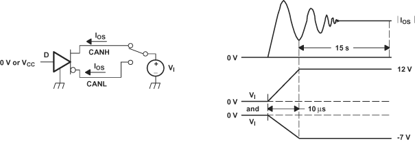 Figure 24. IOS Test Circuit and Waveforms
All input pulses are supplied by a generator with f ≤ 1.5 MHz.
Figure 25. Common-Mode Voltage Rejection