SLLS933G November 2008 – January 2015 SN65HVD233-HT
PRODUCTION DATA.
- 1 Features
- 2 Applications
- 3 Description
- 4 Revision History
- 5 Description (Continued)
- 6 Pin Configuration and Functions
-
7 Specifications
- 7.1 Absolute Maximum Ratings
- 7.2 ESD Ratings
- 7.3 Recommended Operating Conditions
- 7.4 Thermal Information
- 7.5 Driver Electrical Characteristics
- 7.6 Receiver Electrical Characteristics
- 7.7 Driver Switching Characteristics
- 7.8 Receiver Switching Characteristics
- 7.9 Device Switching Characteristics
- 7.10 Typical Characteristics
- 8 Parameter Measurement Information
- 9 Detailed Description
- 10Application and Implementation
- 11Power Supply Recommendations
- 12Layout
- 13Device and Documentation Support
- 14Mechanical, Packaging, and Orderable Information
封装选项
机械数据 (封装 | 引脚)
散热焊盘机械数据 (封装 | 引脚)
订购信息
10 Application and Implementation
NOTE
Information in the following applications sections is not part of the TI component specification, and TI does not warrant its accuracy or completeness. TI’s customers are responsible for determining suitability of components for their purposes. Customers should validate and test their design implementation to confirm system functionality.
10.1 Application Information
10.1.1 Diagnostic Loopback
The loopback (LBK) function of the SN65HVD233 is enabled with a high-level input to pin 5. This forces the driver into a recessive state and redirects the data (D) input at pin 1 to the received-data (R) output at pin 4. This allows the host controller to input and read back a bit sequence to perform diagnostic routines without disturbing the CAN bus. A typical CAN bus application is displayed in Figure 34.
If the LBK pin is not used, it may be tied to ground (GND). However, it is pulled low internally (defaults to a low-level input) and may be left open if not in use.
10.2 Typical Application
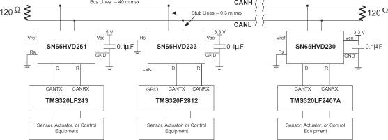 Figure 34. Typical SN65HVD233 Application
10.2.1 Design Requirements
The High-Speed ISO 11898 Standard specifications are given for a maximum signaling rate of 1 Mbps with a bus length of 40 m and a maximum of 30 nodes. It also recommends a maximum un-terminated stub length of 0.3 m. The cable is specified to be a shielded or unshielded twisted-pair with a 120-W characteristic impedance (ZO). The Standard defines a single line of twisted-pair cable with the network topology as shown in Figure 34. It is terminated at both ends with 120-W resistors, which match the characteristic impedance of the line to prevent signal reflections. According to ISO 11898, placing RL on a node should be avoided because the bus lines lose termination if the node is disconnected from the bus.
10.2.2 Detailed Design Procedure
Table 5. Suggested Cable Length vs Signaling Rate
| BUS LENGTH (m) | SIGNALING RATE (Mbps) |
|---|---|
| 40 | 1 |
| 100 | 0.5 |
| 200 | 0.25 |
| 500 | 0.10 |
| 1000 | 0.05 |
Basically, the maximum bus length is determined by, or rather is a trade-off with the selected signaling rate as listed in Table 5.
A signaling rate decreases as transmission distance increases. While steady-state losses may become a factor at the longest transmission distances, the major factors limiting signaling rate as distance is increased are time varying. Cable bandwidth limitations, which degrade the signal transition time and introduce inter-symbol interference (ISI), are primary factors reducing the achievable signaling rate when transmission distance is increased.
For a CAN bus, the signaling rate is also determined from the total system delay – down and back between the two most distant nodes of a system and the sum of the delays into and out of the nodes on a bus with the typical 5ns/m prop delay of a twisted-pair cable. Also, consideration must be given the signal amplitude loss due to resistance of the cable and the input resistance of the transceivers. Under strict analysis, skin effects, proximity to other circuitry, dielectric loss, and radiation loss effects all act to influence the primary line parameters and degrade the signal.
A conservative rule of thumb for bus lengths over 100 m is derived from the product of the signaling rate in Mbps and the bus length in meters, which should be less than or equal to 50.
Signaling Rate (Mbps) × Bus Length (m) <= 50. Operation at extreme temperatures should employ additional conservatism.
10.2.2.1 Slope Control
The rise and fall slope of the SN65HVD233 driver output can be adjusted by connecting a resistor from Rs (pin 8) to ground (GND), or to a low-level input voltage (see Figure 35).
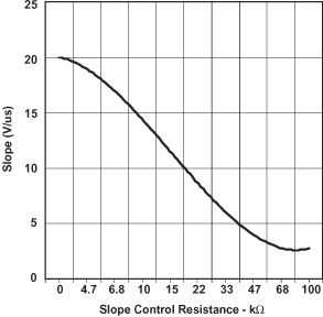
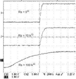
The slope of the driver output signal is proportional to the output current of the pin. This slope control is implemented with an external resistor value of 10 kΩ to achieve a ≉15-V/μs slew rate, and up to 100 kΩ to achieve a ≉2.0- V/μs slew rate (see Figure 36). Typical driver output waveforms with slope control are displayed in Figure 37.
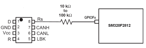 Figure 35. Slope Control/Standby Connection to DSP
10.2.2.2 Standby
If a high-level input (>0.75 VCC) is applied to Rs, the circuit enters a low-current, listen-only standby mode, during which the driver is switched off and the receiver remains active. The local controller can reverse this low-power standby mode when the rising edge of a dominant state (bus differential voltage >900 mV typical) occurs on the bus.
10.2.3 Application Curves