SLLS934F November 2008 – November 2015 SN65HVD11-HT
PRODUCTION DATA.
- 1 Features
- 2 Applications
- 3 Description
- 4 Revision History
- 5 Pin Configuration and Functions
- 6 Specifications
- 7 Parameter Measurement Information
- 8 Detailed Description
- 9 Application and Implementation
- 10Power Supply Recommendations
- 11Layout
- 12Device and Documentation Support
- 13Mechanical, Packaging, and Orderable Information
封装选项
机械数据 (封装 | 引脚)
散热焊盘机械数据 (封装 | 引脚)
订购信息
11 Layout
11.1 Layout Guidelines
On-chip IEC-ESD protection is sufficient for laboratory and portable equipment but never sufficient for EFT and surge transients occurring in industrial environments. Therefore, robust and reliable bus node design requires the use of external transient protection devices.
Because ESD and EFT transients have a wide frequency bandwidth from approximately 3 MHz to 3 GHz, high-frequency layout techniques must be applied during PCB design.
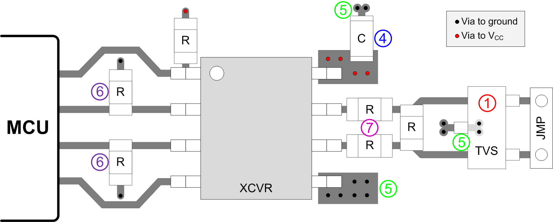
- Place the protection circuitry close to the bus connector to prevent noise transients from entering the board.
- Use VCC and ground planes to provide low-inductance. High-frequency currents follow the path of least inductance and not the path of least impedance.
- Design the protection components into the direction of the signal path. Do not force the transient currents to divert from the signal path to reach the protection device.
- Apply 100-nF to 220-nF bypass capacitors as close as possible to the VCC pins of transceiver, UART, and controller ICs on the board.
- Use at least two vias for VCC and ground connections of bypass capacitors and protection devices to minimize effective via-inductance.
- Use 1-kΩ to 10-kΩ pullup or pulldown resistors for enable lines to limit noise currents in these lines during transient events.
- Insert pulse-proof series resistors into the A and B bus lines if the TVS clamping voltage is higher than the specified maximum voltage of the transceiver bus terminals. These resistors limit the residual clamping current into the transceiver and prevent it from latching up.
- While pure TVS protection is sufficient for surge transients up to 1 kV, higher transients require metal-oxide varistors (MOVs) which reduce the transients to a few hundred volts of clamping voltage, and transient blocking units (TBUs) that limit transient current to less than 1 mA.
11.2 Layout Example
 Figure 27. SN65HVD11-HT Layout Example
11.3 Thermal Considerations
RθJA (Junction-to-Ambient Thermal Resistance) is defined as the difference in junction temperature to ambient temperature divided by the operating power.
RθJA is not a constant and is a strong function of:
- the PCB design (50% variation)
- altitude (20% variation)
- device power (5% variation)
RθJA can be used to compare the thermal performance of packages if the specific test conditions are defined and used. Standardized testing includes specification of PCB construction, test chamber volume, sensor locations, and the thermal characteristics of holding fixtures. θJA is often misused when it is used to calculate junction temperatures for other installations.
TI uses two test PCBs as defined by JEDEC specifications. The low-k board gives average in-use condition thermal performance, and it consists of a single copper trace layer 25-mm long and 2-oz thick. The high-k board gives best case in-use condition, and it consists of two 1-oz buried power planes with a single copper trace layer 25-mm long and 2-oz thick. A 4% to 50% difference in θJA can be measured between these two test cards.
RθJC (Junction-to-Case Thermal Resistance) is defined as difference in junction temperature to case divided by the operating power. It is measured by putting the mounted package up against a copper block cold plate to force heat to flow from die, through the mold compound into the copper block.
RθJC is a useful thermal characteristic when a heatsink is applied to package. It is not a useful characteristic to predict junction temperature because it provides pessimistic numbers if the case temperature is measured in a nonstandard system and junction temperatures are backed out. It can be used with θJB in 1-dimensional thermal simulation of a package system.
RθJB (Junction-to-Board Thermal Resistance) is defined as the difference in the junction temperature and the PCB temperature at the center of the package (closest to the die) when the PCB is clamped in a cold-plate structure. θJB is only defined for the high-k test card.
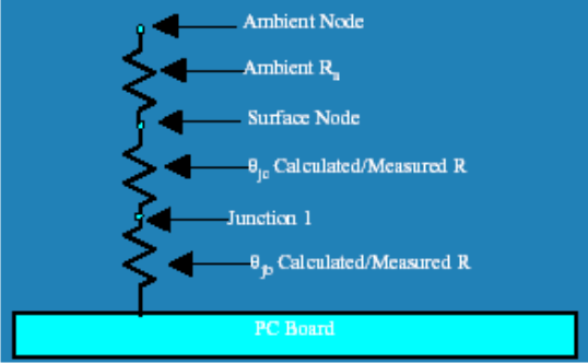
RθJB provides an overall thermal resistance between the die and the PCB. It includes a bit of the PCB thermal resistance (especially for BGA’s with thermal balls) and can be used for simple 1-dimensional network analysis of package system, see Figure 28.
 Figure 28. Thermal Resistance