SBOS502F September   2009  – December 2016 REF5025-HT

PRODUCTION DATA.  

  1. Features
  2. Applications
  3. Description
  4. Revision History
  5. Pin Configuration and Functions
  6. Specifications
    1. 6.1 Absolute Maximum Ratings
    2. 6.2 ESD Ratings
    3. 6.3 Recommended Operating Conditions
    4. 6.4 Thermal Information
    5. 6.5 Electrical Characteristics
    6. 6.6 Typical Characteristics
  7. Detailed Description
    1. 7.1 Overview
    2. 7.2 Functional Block Diagram
    3. 7.3 Feature Description
      1. 7.3.1 Output Adjustment Using the TRIM/NR Pin
      2. 7.3.2 Low Temperature Drift
      3. 7.3.3 Temperature Monitoring
      4. 7.3.4 Noise Performance
    4. 7.4 Device Functional Modes
  8. Application and Implementation
    1. 8.1 Application Information
    2. 8.2 Typical Applications
      1. 8.2.1 Negative Reference Voltage
        1. 8.2.1.1 Design Requirements
        2. 8.2.1.2 Detailed Design Procedure
        3. 8.2.1.3 Application Curves
      2. 8.2.2 Positive Reference Voltage
        1. 8.2.2.1 Detailed Design Procedure
          1. 8.2.2.1.1 Load Capacitance
          2. 8.2.2.1.2 Bandgap Noise Reduction
    3. 8.3 System Example
      1. 8.3.1 Data Acquisition
  9. Power Supply Recommendations
  10. 10Layout
    1. 10.1 Layout Guidelines
    2. 10.2 Layout Example
    3. 10.3 Power Dissipation
  11. 11Device and Documentation Support
    1. 11.1 Documentation Support
      1. 11.1.1 Related Documentation
    2. 11.2 Receiving Notification of Documentation Updates
    3. 11.3 Community Resources
    4. 11.4 Trademarks
    5. 11.5 Electrostatic Discharge Caution
    6. 11.6 Glossary
  12. 12Mechanical, Packaging, and Orderable Information

封装选项

机械数据 (封装 | 引脚)
散热焊盘机械数据 (封装 | 引脚)
订购信息

Power Supply Recommendations

The minimum recommended power supply voltage for REF5025-HT is 3.25 V. The maximum power supply voltage for the REF5025-HT is 18 V. TI recommends adding a bypass capacitor of 1 μF to 10 μF at the input to compensate for the layout and power supply source impedance.

Figure 36 shows the typical connections for the REF5025-HT. TI recommends a supply bypass capacitor with a value ranging from 1 μF to 10 μF. A 1-μF to 50-μF output capacitor (CL) must be connected from VOUT to GND. The ESR value of CL must be less than or equal to 1.5-Ω to ensure output stability. To minimize noise, TI recommends the ESR value of the of CL is between 1-Ω and 1.5-Ω.
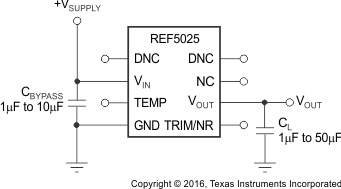
REF5025-HT ai_basic_conn_bos502.gif Figure 36. Basic Connections