SBVS299 April 2017
PRODUCTION DATA.
- 1 Features
- 2 Applications
- 3 Description
- 4 Revision History
- 5 Device Comparison Table
- 6 Pin Configuration and Functions
- 7 Specifications
- 8 Detailed Description
- 9 Application and Implementation
- 10Power Supply Recommendations
- 11Layout
- 12Device and Documentation Support
- 13Mechanical, Packaging, and Orderable Information
1 Features
- AEC-Q100 Qualified With the Following Results:
- Device TA Range: –40°C to 125°C
- Device HBM ESD Classification Level H1C
- Device CDM ESD Classification Level C4A
- High Accuracy: 0.2% Maximum
- Excellent Specified Drift Performance:
- 20 ppm/°C (Maximum) from –40°C to +125°C
- High Output Current: ±10 mA
- Low Dropout: 5 mV
- Low IQ: 115 µA Maximum
- Low Noise: 17 µVp-p/V
- No Output Capacitor Required
- Available Voltage Options : 1.2 V, 2 V, 2.5 V, 3 V, 3.3 V, 4 V
- MicroSize Package: 3-Pin SOT-23
2 Applications
- HEV/EV Powertrain Systems
- Automotive Battery Management Systems
- Inverter
- Electric Power Steering Systems
- Advanced Driver Assistance Systems (ADAS)
- Radar Systems
- Night Vision Systems
- Dynamic Spotlight
- Front Camera
- Infotainment MCU Attached
- Portable, Battery-Powered Equipment
3 Description
The REF31xx-Q1 is a family of precision, low power, low dropout, series voltage references available in the tiny 3-pin SOT-23 package.
The REF31xx-Q1 small size and low power consumption (100 μA typical) make it ideal for portable and battery-powered applications. The REF31xx-Q1 does not require a load capacitor, but is stable with any capacitive load and can sink or source up to 10 mA of output current.
Unloaded, the REF31xx-Q1 can operate on supplies down to 5 mV above the output voltage. All models are specified for the wide temperature range of –40°C to +125°C.
Device Information(1)
| PART NUMBER | PACKAGE | BODY SIZE (NOM) |
|---|---|---|
| REF3112-Q1 REF3120-Q1 REF3125-Q1 REF3130-Q1 REF3133-Q1 REF3140-Q1 |
SOT-23 (3) | 2.92 mm × 1.30 mm |
- For all available packages, see the orderable addendum at the end of the data sheet.
SPACER
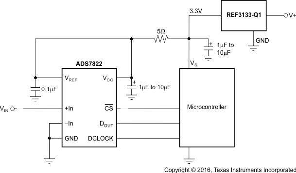
Typical Application

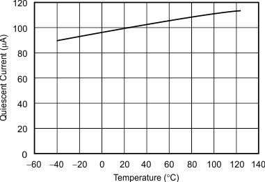
Quiescent Current vs Temperature
