ZHCSGP1 September   2017 REF2125

PRODUCTION DATA.  

  1. 特性
  2. 应用
  3. 说明
  4. 修订历史记录
  5. Pin Configuration and Functions
  6. Specifications
    1. 6.1 Absolute Maximum Ratings
    2. 6.2 ESD Ratings
    3. 6.3 Recommended Operating Conditions
    4. 6.4 Thermal Information
    5. 6.5 Electrical Characteristics
    6. 6.6 Typical Characteristics
  7. Parameter Measurement Information
    1. 7.1 Solder Heat Shift
    2. 7.2 Long-Term Stability
    3. 7.3 Thermal Hysteresis
    4. 7.4 Power Dissipation
    5. 7.5 Noise Performance
  8. Detailed Description
    1. 8.1 Overview
    2. 8.2 Functional Block Diagram
    3. 8.3 Feature Description
      1. 8.3.1 Supply Voltage
      2. 8.3.2 Low Temperature Drift
      3. 8.3.3 Load Current
      4. 8.3.4 Clean Start Feature
    4. 8.4 Device Functional Modes
      1. 8.4.1 EN Pin
      2. 8.4.2 Negative Reference Voltage
  9. Applications and Implementation
    1. 9.1 Application Information
    2. 9.2 Typical Application: Basic Voltage Reference Connection
      1. 9.2.1 Design Requirements
      2. 9.2.2 Detailed Design Procedure
        1. 9.2.2.1 Input and Output Capacitors
        2. 9.2.2.2 VIN Slew Rate Considerations
        3. 9.2.2.3 Shutdown/Enable Feature
      3. 9.2.3 Application Curves
  10. 10Power-Supply Recommendations
  11. 11Layout
    1. 11.1 Layout Guidelines
    2. 11.2 Layout Example
  12. 12器件和文档支持
    1. 12.1 文档支持
      1. 12.1.1 相关文档
    2. 12.2 接收文档更新通知
    3. 12.3 社区资源
    4. 12.4 商标
    5. 12.5 静电放电警告
    6. 12.6 Glossary
  13. 13机械、封装和可订购信息

封装选项

机械数据 (封装 | 引脚)
散热焊盘机械数据 (封装 | 引脚)
订购信息

Pin Configuration and Functions

DBV Package
5-Pin SOT-23
Top View
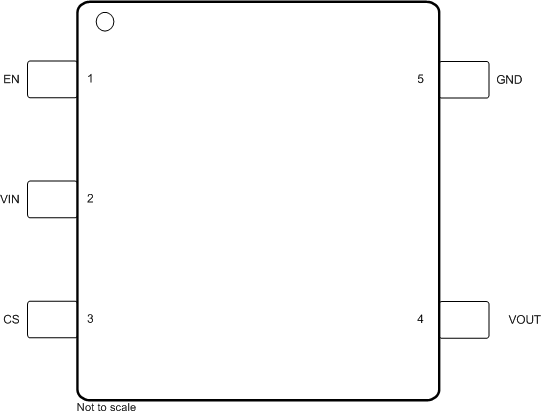
REF2125 pinout_3.gif

Pin Functions

PIN TYPE DESCRIPTION
NO. NAME
1 EN Input Enable connection. Enables or disables the device.
2 VIN Power Input supply voltage connection.
3 CS Input Clean start pin. Connect to a resistor or capacitor to enable the clean start feature.
4 VOUT Output Reference voltage output.
5 GND Ground Ground connection.