ZHCSA60C May   2012  – May 2015 PCM5100A , PCM5100A-Q1 , PCM5101A , PCM5101A-Q1 , PCM5102A , PCM5102A-Q1

PRODUCTION DATA.  

  1. 特性
  2. 应用
  3. 说明
  4. 简化系统图
  5. 修订历史记录
  6. Device Comparison
  7. Pin Configuration and Functions
  8. Specifications
    1. 8.1 Absolute Maximum Ratings
    2. 8.2 ESD Ratings Updated ESD Data
    3. 8.3 Recommended Operating Conditions
    4. 8.4 Thermal Information
    5. 8.5 Electrical Characteristics
    6. 8.6 Timing Requirements
    7. 8.7 Timing Requirements, XSMT
    8. 8.8 Typical Characteristics
  9. Detailed Description
    1. 9.1 Overview
    2. 9.2 Functional Block Diagram
    3. 9.3 Feature Description
      1. 9.3.1 Terminology
      2. 9.3.2 Audio Data Interface
        1. 9.3.2.1 Audio Serial Interface
        2. 9.3.2.2 PCM Audio Data Formats
        3. 9.3.2.3 Zero Data Detect
      3. 9.3.3 XSMT Pin (Soft Mute / Soft Un-Mute)
      4. 9.3.4 Audio Processing
        1. 9.3.4.1 Interpolation Filter
      5. 9.3.5 Reset and System Clock Functions
        1. 9.3.5.1 Clocking Overview
        2. 9.3.5.2 Clock Slave Mode With Master/System Clock (SCK) Input (4 Wire I2S)
        3. 9.3.5.3 Clock Slave Mode with BCK PLL to Generate Internal Clocks (3-Wire PCM)
    4. 9.4 Device Functional Modes
      1. 9.4.1 External SCK and PLL Activation
        1. 9.4.1.1 Interpolation Filter Modes
        2. 9.4.1.2 44.1kHz De-emphasis
        3. 9.4.1.3 Audio Format
  10. 10Applications and Implementation
    1. 10.1 Application Information
      1. 10.1.1 Typical Applications
        1. 10.1.1.1 Example Design Requirements
        2. 10.1.1.2 Detailed Design Procedure
        3. 10.1.1.3 Application Curve
  11. 11Power Supply Recommendations
    1. 11.1 Power Supply Distribution and Requirements
    2. 11.2 Recommended Powerdown Sequence
      1. 11.2.1 Planned Shutdown
      2. 11.2.2 Unplanned Shutdown
    3. 11.3 External Power Sense Undervoltage Protection Mode
    4. 11.4 Power-On Reset Function
    5. 11.5 PCM510xA Power Modes
      1. 11.5.1 Setting Digital Power Supplies and I/O Voltage Rails
      2. 11.5.2 Power Save Modes
  12. 12Layout
    1. 12.1 Layout Guidelines
  13. 13器件和文档支持
    1. 13.1 相关链接
    2. 13.2 社区资源
    3. 13.3 商标
    4. 13.4 静电放电警告
  14. 14机械、封装和可订购信息
    1. 14.1 机械数据

封装选项

机械数据 (封装 | 引脚)
散热焊盘机械数据 (封装 | 引脚)
订购信息

12 Layout

12.1 Layout Guidelines

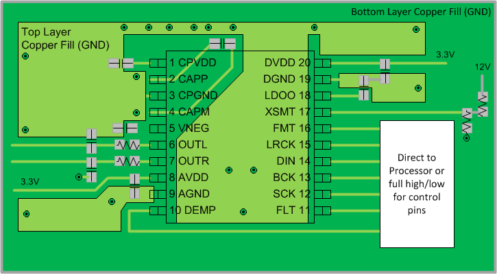
  • The PCM510xA family of devices are simple to layout. Most engineers use a shared common ground for an entire device. GND can be consider AGND and DGND connected.
  • Good system partitioning should keep digital clock and interface traces away from the analog outputs for highest analog performance. This reduces any high speed clock return currents influencing the analog outputs.
  • Power supply and charge pump decoupling capacitors should be placed as close as possible to the device.
  • The top layer should be used for routing signals, whilst the bottom layer can be used for GND.
PCM5100A PCM5101A PCM5102A PCM5100A-Q1 PCM5101A-Q1 PCM5102A-Q1 PCM510x_layout_recommendation.gif Figure 43. PCM510x Layout Example