ZHCSGE9 July 2017 OPA196 , OPA2196 , OPA4196
PRODUCTION DATA.
- 1 特性
- 2 应用
- 3 说明
- 4 修订历史记录
- 5 Pin Configuration and Functions
-
6 Specifications
- 6.1 Absolute Maximum Ratings
- 6.2 ESD Ratings
- 6.3 Recommended Operating Conditions
- 6.4 Thermal Information: OPA196
- 6.5 Thermal Information: OPA2196
- 6.6 Thermal Information: OPA4196
- 6.7 Electrical Characteristics: VS = ±4 V to ±18 V (VS = 8 V to 36 V)
- 6.8 Electrical Characteristics: VS = ±2.25 V to ±4 V (VS = 4.5 V to 8 V)
- 6.9 Typical Characteristics
- 7 Detailed Description
- 8 Application and Implementation
- 9 Power-Supply Recommendations
- 10Layout
- 11器件和文档支持
- 12机械、封装和可订购信息
5 Pin Configuration and Functions
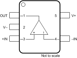
DBV Package: OPA196
5-Pin SOT
Top View

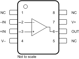
D and DGK Packages: OPA196
8-Pin SOIC and VSSOP
Top View

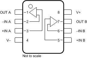
D and DGK Packages: OPA2196
8-Pin SOIC and VSSOP
Top View

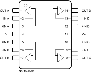
D and PW Packages: OPA4196
14-Pin SOIC and TSSOP
Top View

1. NC = No internal connection.
Pin Functions: OPA196
| PIN | I/O | DESCRIPTION | ||
|---|---|---|---|---|
| NAME | OPA196 | |||
| D (SOIC), DGK (VSSOP) |
DBV (SOT) | |||
| +IN | 3 | 3 | I | Noninverting input |
| –IN | 2 | 4 | I | Inverting input |
| NC | 1, 5, 8 | — | — | No internal connection (can be left floating) |
| OUT | 6 | 1 | O | Output |
| V+ | 7 | 5 | — | Positive (highest) power supply |
| V– | 4 | 2 | — | Negative (lowest) power supply |
Pin Functions: OPA2196 and OPA4196
| PIN | I/O | DESCRIPTION | ||
|---|---|---|---|---|
| NAME | OPA2196 | OPA4196 | ||
| D (SOIC), DGK (VSSOP) |
D (SOIC), PW (TSSOP) |
|||
| +IN A | 3 | 3 | I | Noninverting input, channel A |
| +IN B | 5 | 5 | I | Noninverting input, channel B |
| +IN C | — | 10 | I | Noninverting input, channel C |
| +IN D | — | 12 | I | Noninverting input, channel D |
| –IN A | 2 | 2 | I | Inverting input, channel A |
| –IN B | 6 | 6 | I | Inverting input, channel B |
| –IN C | — | 9 | I | Inverting input,,channel C |
| –IN D | — | 13 | I | Inverting input, channel D |
| OUT A | 1 | 1 | O | Output, channel A |
| OUT B | 7 | 7 | O | Output, channel B |
| OUT C | — | 8 | O | Output, channel C |
| OUT D | — | 14 | O | Output, channel D |
| V+ | 8 | 4 | — | Positive (highest) power supply |
| V– | 4 | 11 | — | Negative (lowest) power supply |