SBOS483I July 2009 – May 2015 OPA2333-HT
PRODUCTION DATA.
- 1 Features
- 2 Applications
- 3 Description
- 4 Revision History
- 5 Pin Configuration and Functions
- 6 Specifications
- 7 Detailed Description
- 8 Application and Implementation
- 9 Power Supply Recommendations
- 10Layout
- 11Device and Documentation Support
- 12Mechanical, Packaging, and Orderable Information
封装选项
机械数据 (封装 | 引脚)
散热焊盘机械数据 (封装 | 引脚)
订购信息
6 Specifications
6.1 Absolute Maximum Ratings
over operating free-air temperature range (unless otherwise noted)(1)| MIN | MAX | UNIT | ||
|---|---|---|---|---|
| Supply voltage | 7 | V | ||
| Signal input terminals, voltage(2) | –0.3 | (V+) + 0.3 | V | |
| Output short circuit(3) | Continuous | |||
| Operating temperature | JD, HKJ, HKQ packages | –55 | 210 | °C |
| D package | –55 | 175 | ||
| Junction temperature | JD, HKJ, HKQ packages | 210 | °C | |
| D package | 175 | |||
| Storage temperature, Tstg | –65 | 210 | °C | |
(1) Stresses beyond those listed under Absolute Maximum Ratings may cause permanent damage to the device. These are stress ratings only, which do not imply functional operation of the device at these or any other conditions beyond those indicated under Recommended Operating Conditions. Exposure to absolute-maximum-rated conditions for extended periods may affect device reliability.
(2) Input terminals are diode clamped to the power-supply rails. Input signals that can swing more than 0.3 V beyond the supply rails should be current limited to 10 mA or less.
(3) Short circuit to ground, one amplifier per package.
6.2 ESD Ratings
| VALUE | UNIT | |||
|---|---|---|---|---|
| V(ESD) | Electrostatic discharge | Human body model (HBM), per ANSI/ESDA/JEDEC JS-001(1) | ±4000 | V |
| Charged-device model (CDM), per JEDEC specification JESD22-C101(2) | ±1000 | |||
(1) JEDEC document JEP155 states that 500-V HBM allows safe manufacturing with a standard ESD control process.
(2) JEDEC document JEP157 states that 250-V CDM allows safe manufacturing with a standard ESD control process.
6.3 Recommended Operating Conditions
over operating free-air temperature range (unless otherwise noted)| MIN | NOM | MAX | UNIT | ||
|---|---|---|---|---|---|
| Supply voltage, VS = (V+) – (V–) | 1.8 (±0.9) | 5 (±2.5) | 5.5 (±2.75) | V | |
| Operating temperature | JD, HKJ, HKQ packages | –55 | 210 | °C | |
| D package | –55 | 175 | |||
6.4 Thermal Information
| THERMAL METRIC(1) | OPA2333-HT | UNIT | |||||
|---|---|---|---|---|---|---|---|
| JD (CDIP SB) |
HKJ (CFP) |
HKQ (CFP) |
D (SOIC) |
||||
| 8 PINS | 8 PINS | 8 PINS | 8 PINS | ||||
| RθJA | Junction-to-ambient thermal resistance(2) | High-K board(3), no airflow | — | — | — | 117.5 | °C/W |
| No airflow | — | — | — | — | |||
| RθJC(top) | Junction-to-case (top) thermal resistance | 53.8 | 57.7 | 62.0 | °C/W | ||
| to ceramic side of case | — | — | 15.2 | — | |||
| to top of case lid (metal side of case) | — | — | — | — | |||
| RθJB | Junction-to-board thermal resistance | High-K board without underfill | 76.0 | 61.0 | 151.6 | 57.7 | °C/W |
| ψJT | Junction-to-top characterization parameter | — | — | — | 19.4 | °C/W | |
| ψJB | Junction-to-board characterization parameter | — | — | — | 57.2 | °C/W | |
| RθJC(bot) | Junction-to-case (bottom) thermal resistance | 26.7 | 15.2 | 56.9 | — | °C/W | |
(1) For more information about traditional and new thermal metrics, see the Semiconductor and IC Package Thermal Metrics application report, SPRA953.
(2) The intent of RθJA specification is solely for a thermal performance comparison of one package to another in a standardized environment.
This methodology is not meant to and will not predict the performance of a package in an application-specific environment.
This methodology is not meant to and will not predict the performance of a package in an application-specific environment.
(3) JED51-7, high effective thermal conductivity test board for leaded surface mount packages
6.5 Electrical Characteristics
VS = 1.8 V to 5.5 V, TA = 25°C, RL = 10 kΩ connected to VS/2, VCM = VS/2, and VOUT = VS/2 (unless otherwise noted).| PARAMETER | TEST CONDITIONS | MIN | TYP | MAX | UNIT | ||
|---|---|---|---|---|---|---|---|
| OFFSET VOLTAGE | |||||||
| VOS | Input offset voltage | VS = 5 V | TA = 25°C | 2 | 10 | μV | |
| TA = –55°C to 125°C | 22 | ||||||
| TA = –55°C to 175°C(1) | 26 | ||||||
| TA = –55°C to 210°C(2) | 26 | μV | |||||
| dVOS/dT | Input Offset Voltage Temperature Drift | VS = 5 V | TA = –55°C to 125°C | 0.02 | μV/°C | ||
| TA = –55°C to 175°C(1) | 0.05 | ||||||
| TA = –55°C to 210°C(2) | 0.05 | ||||||
| PSRR | Input Offset Voltage vs Power Supply | VS = 1.8 V to 5.5 V | TA = –55°C to 125°C | 1 | 6 | μV/V | |
| TA = –55°C to 175°C(1) | 1.2 | 8 | |||||
| TA = –55°C to 210°C(2) | 1.7 | 11 | |||||
| INPUT BIAS CURRENT | |||||||
| IB | Input bias current | TA = 25°C | ±70 | ±200 | pA | ||
| TA = –55°C to 125°C | ±150 | ||||||
| TA = –55°C to 175°C | ±1250 | ||||||
| TA = –55°C to 210°C | ±5300 | ||||||
| IOS | Input offset current | TA = –55°C to 125°C | ±140 | ±400 | pA | ||
| TA = –55°C to 175°C | ±700 | ||||||
| TA = –55°C to 210°C | ±10600 | ||||||
| NOISE | |||||||
| Input Noise Voltage | f = 0.01 Hz to 1 Hz | TA = –55°C to 125°C | 0.3 | μVPP | |||
| TA = –55°C to 175°C(1) | 1 | ||||||
| TA = –55°C to 210°C(2) | 1 | ||||||
| f = 0.1 Hz to 10 Hz | TA = –55°C to 125°C | 1.1 | μVPP | ||||
| TA = –55°C to 175°C(1) | 1.5 | ||||||
| TA = –55°C to 210°C(2) | 1.5 | ||||||
| in | Input Noise Current Density | f = 10 Hz | TA = 25°C | 100 | fA/√Hz | ||
| INPUT VOLTAGE RANGE(3) | |||||||
| VCM | Common mode voltage range | TA = –55°C to 125°C | (V–) – 0.1 | (V+) + 0.1 | V | ||
| TA = –55°C to 175°C | (V–) – 0.25 | (V+) + 0.25 | |||||
| TA = –55°C to 210°C | (V–) – 0.25 | (V+) + 0.25 | |||||
| CMRR | Common-Mode Rejection Ratio | (V–) – 0.1 V < VCM < (V+) + 0.1 V | TA = –55°C to 125°C | 102 | 130 | dB | |
| TA = –55°C to 175°C | 101 | ||||||
| TA = –55°C to 210°C | 91 | ||||||
| INPUT CAPACITANCE | |||||||
| Differential | TA = –55°C to 125°C | 2 | pF | ||||
| TA = –55°C to 175°C | 4.25 | ||||||
| TA = –55°C to 210°C | 4.25 | ||||||
| Common mode | TA = –55°C to 125°C | 4 | pF | ||||
| TA = –55°C to 175°C | 12.25 | ||||||
| TA = –55°C to 210°C | 12.25 | ||||||
| OPEN-LOOP GAIN | |||||||
| AOL | Open-loop voltage gain | (V–) + 100 mV < VO < (V+) – 100 mV, RL = 10 kΩ | TA = –55°C to 125°C | 104 | 130 | dB | |
| TA = –55°C to 175°C(1) | 93 | 110 | |||||
| TA = –55°C to 210°C(2) | 85 | 93 | |||||
| FREQUENCY RESPONSE | |||||||
| GBW | Gain-bandwidth product | CL = 100 pF | TA = –55°C to 125°C | 350 | kHz | ||
| TA = –55°C to 175°C | 350 | ||||||
| TA = –55°C to 210°C | 350 | ||||||
| SR | Slew rate | G = 1 | TA = –55°C to 125°C | 0.16 | V/μs | ||
| TA = –55°C to 175°C | 0.25 | ||||||
| TA = –55°C to 210°C | 0.25 | ||||||
| OUTPUT | |||||||
| Voltage output swing from rail | RL = 10 kΩ | TA = 25°C | 30 | 50 | mV | ||
| TA = –55°C to 125°C | 85 | ||||||
| TA = –55°C to 175°C(1) | 110 | ||||||
| TA = –55°C to 210°C(2) | 150 | ||||||
| ISC | Short-circuit current | TA = 25°C | ±5 | mA | |||
| Open-loop output impedance(4) | f = 350 kHz, IO = 0 | 2 | kΩ | ||||
| POWER SUPPLY | |||||||
| VS | Specified voltage range | TA = –55°C to 210°C(2) | 1.8 | 5.5 | V | ||
| IQ | Quiescent current per amplifier | IO = 0 | TA = 25°C | 17 | 25 | μA | |
| TA = –55°C to 125°C | 30 | ||||||
| TA = –55°C to 175°C(1) | 35 | 40 | |||||
| TA = –55°C to 210°C(2) | 50 | 80 | |||||
| Turnon time | VS = 5 V | TA = 25°C | 100 | μs | |||
(1) Minimum and maximum parameters are characterized for operation at TA = 175°C, but may not be production tested at that temperature. Production test limits with statistical guardbands are used to ensure high temperature performance.
(2) Minimum and maximum parameters are characterized for operation at TA = 210°C, but may not be production tested at that temperature. Production test limits with statistical guardbands are used to ensure high temperature performance.
(3) The OPA2333-HT is not intended to be used as a comparator due to its limited differential input range capability.
(4) See Typical Characteristics.
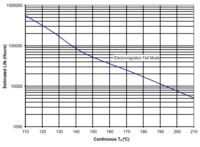
1. See datasheet for absolute maximum and minimum recommended operating conditions.
2. Silicon operating life design goal is 10 years at 105°C junction temperature (does not include package interconnect life).
3. The predicted operating lifetime vs. junction temperature is based on reliability modeling using electromigration as the dominant failure mechanism affecting device wearout for the specific device process and design characteristics.
4. This device is qualified for 1000 hours of continuous operation at maximum rated temperature.
Figure 1. OPA2333SKGD1 and OPA2333HD Operating Life Derating Chart
6.6 Typical Characteristics
At TA = 25°C, VS = 5 V, and CL = 0 pF (unless otherwise noted).
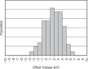 Figure 2. Offset Voltage Production Distribution
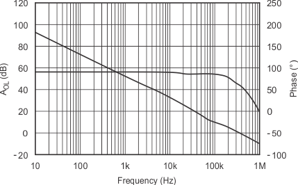 Figure 4. Open−Loop Gain vs Frequency
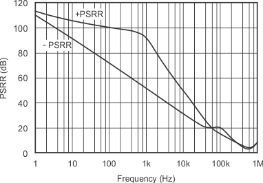 Figure 6. PSRR vs Frequency
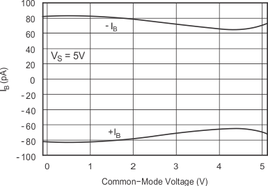 Figure 8. Input Bias Current vs Common−Mode Voltage
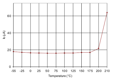 Figure 10. Quiescent Current vs Temperature
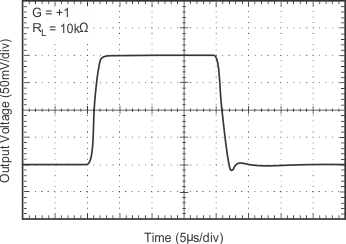 Figure 12. Small−Signal Step Response
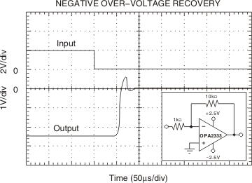 Figure 14. Negative Overvoltage Recovery
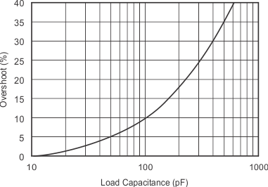 Figure 16. Small−Signal Overshoot vs Load Capacitance
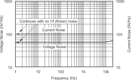 Figure 18. Current and Voltage Noise Spectral Density vs Frequency
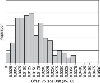 Figure 3. Offset Voltage Drift Production Distribution
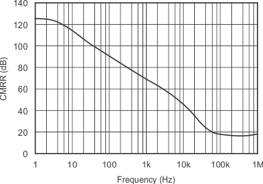 Figure 5. CMMR vs Frequency
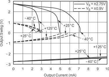 Figure 7. Output Voltage Swing vs Output Current
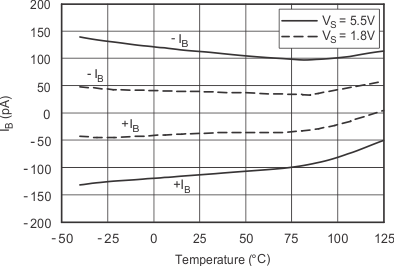 Figure 9. Input Bias Current vs Temperature
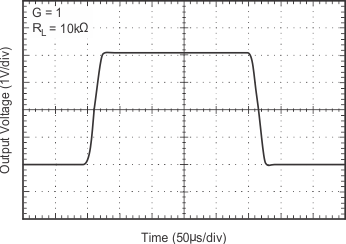 Figure 11. Large−Signal Step Response
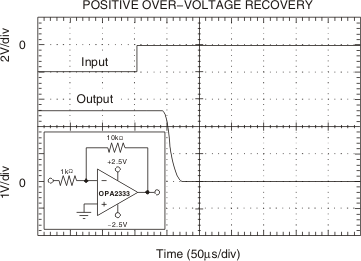 Figure 13. Positive Overvoltage Recovery
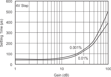 Figure 15. Settling Time vs Closed−Loop Gain
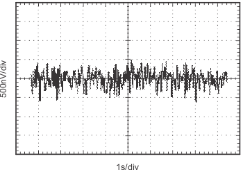 Figure 17. 0.1-Hz to 10-Hz Noise