ZHCSEE5B November   2015  – May 2016 OPA1622

PRODUCTION DATA.  

  1. 特性
  2. 应用
  3. 说明
  4. 修订历史记录
  5. Pin Configuration and Functions
  6. Specifications
    1. 6.1 Absolute Maximum Ratings
    2. 6.2 ESD Ratings
    3. 6.3 Recommended Operating Conditions
    4. 6.4 Thermal Information
    5. 6.5 Electrical Characteristics:
    6. 6.6 Typical Characteristics
  7. Detailed Description
    1. 7.1 Overview
    2. 7.2 Functional Block Diagram
    3. 7.3 Feature Description
      1. 7.3.1 Power Dissipation
      2. 7.3.2 Thermal Shutdown
      3. 7.3.3 Enable Pin
      4. 7.3.4 Ground Pin
      5. 7.3.5 Electrical Overstress
      6. 7.3.6 Input Protection
    4. 7.4 Device Functional Modes
      1. 7.4.1 Shutdown Mode
      2. 7.4.2 Output Transients During Power Up and Power Down
  8. Application and Implementation
    1. 8.1 Application Information
      1. 8.1.1 Noise Performance
        1. 8.1.1.1 Noise Calculations
        2. 8.1.1.2 Application Curve
        3. 8.1.1.3 Basic Noise Calculations
      2. 8.1.2 Total Harmonic Distortion Measurements
    2. 8.2 Typical Application
      1. 8.2.1 Design Requirements
      2. 8.2.2 Detailed Design Procedure
      3. 8.2.3 Application Curves
  9. Power Supply Recommendations
  10. 10Layout
    1. 10.1 Layout Guidelines
    2. 10.2 Layout Example
  11. 11器件和文档支持
    1. 11.1 器件支持
      1. 11.1.1 开发支持
        1. 11.1.1.1 TINA-TI(免费软件下载)
        2. 11.1.1.2 TI 高精度设计
    2. 11.2 文档支持
      1. 11.2.1 相关文档 
    3. 11.3 社区资源
    4. 11.4 商标
    5. 11.5 静电放电警告
    6. 11.6 Glossary
  12. 12机械、封装和可订购信息

封装选项

机械数据 (封装 | 引脚)
散热焊盘机械数据 (封装 | 引脚)
订购信息

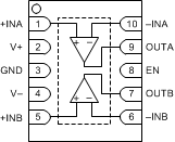
5 Pin Configuration and Functions

DRC Package
10-Pin VSON
Top View
OPA1622 po_drc_sbos727.gif

Pin Functions

PIN I/O DESCRIPTION
NAME NO.
GND 3 Connect to ground
EN 8 I Shutdown (logic low), enable (logic high)
+IN A 1 I Noninverting input, channel A
–IN A 10 I Inverting input, channel A
+IN B 5 I Noninverting input, channel B
–IN B 6 I Inverting input, channel B
OUT A 9 O Output, channel A
OUT B 7 O Output, channel B
V+ 2 Positive (highest) power supply
V– 4 Negative (lowest) power supply
Thermal pad Exposed thermal die pad on underside; connect thermal die pad to V–.
Soldering the thermal pad improves heat dissipation and provides specified performance.