ZHCSEE5B November   2015  – May 2016 OPA1622

PRODUCTION DATA.  

  1. 特性
  2. 应用
  3. 说明
  4. 修订历史记录
  5. Pin Configuration and Functions
  6. Specifications
    1. 6.1 Absolute Maximum Ratings
    2. 6.2 ESD Ratings
    3. 6.3 Recommended Operating Conditions
    4. 6.4 Thermal Information
    5. 6.5 Electrical Characteristics:
    6. 6.6 Typical Characteristics
  7. Detailed Description
    1. 7.1 Overview
    2. 7.2 Functional Block Diagram
    3. 7.3 Feature Description
      1. 7.3.1 Power Dissipation
      2. 7.3.2 Thermal Shutdown
      3. 7.3.3 Enable Pin
      4. 7.3.4 Ground Pin
      5. 7.3.5 Electrical Overstress
      6. 7.3.6 Input Protection
    4. 7.4 Device Functional Modes
      1. 7.4.1 Shutdown Mode
      2. 7.4.2 Output Transients During Power Up and Power Down
  8. Application and Implementation
    1. 8.1 Application Information
      1. 8.1.1 Noise Performance
        1. 8.1.1.1 Noise Calculations
        2. 8.1.1.2 Application Curve
        3. 8.1.1.3 Basic Noise Calculations
      2. 8.1.2 Total Harmonic Distortion Measurements
    2. 8.2 Typical Application
      1. 8.2.1 Design Requirements
      2. 8.2.2 Detailed Design Procedure
      3. 8.2.3 Application Curves
  9. Power Supply Recommendations
  10. 10Layout
    1. 10.1 Layout Guidelines
    2. 10.2 Layout Example
  11. 11器件和文档支持
    1. 11.1 器件支持
      1. 11.1.1 开发支持
        1. 11.1.1.1 TINA-TI(免费软件下载)
        2. 11.1.1.2 TI 高精度设计
    2. 11.2 文档支持
      1. 11.2.1 相关文档 
    3. 11.3 社区资源
    4. 11.4 商标
    5. 11.5 静电放电警告
    6. 11.6 Glossary
  12. 12机械、封装和可订购信息

封装选项

机械数据 (封装 | 引脚)
散热焊盘机械数据 (封装 | 引脚)
订购信息

10 Layout

10.1 Layout Guidelines

For best operational performance of the device, use good printed circuit board (PCB) layout practices, including:

  • Connect low-ESR, 0.1-µF ceramic bypass capacitors between each supply pin and ground, placed as close to the device as possible. A single bypass capacitor from V+ to ground is applicable for single-supply applications. The bypass capacitors are used to reduce the coupled noise by providing low-impedance power sources local to the analog circuitry, because noise can propagate into analog circuitry through the power pins of the circuit as a whole and the op amp specifically.
  • Connect the IC ground pin to a low-impedance, low-noise, system reference point, such as an analog ground.
  • Place the external components as close to the device as possible. As shown in Figure 60, keep feedback resistors close to the inverting input to minimize parasitic capacitance and the feedback loop area.
  • Keep the length of input traces as short as possible. Always remember that the input traces are the most sensitive part of the circuit.
  • For proper amplifier function, connect the package thermal pad to the most negative supply voltage (VEE).

10.2 Layout Example
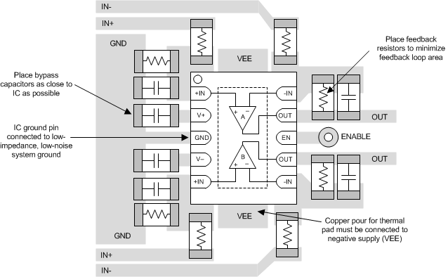
OPA1622 d302_pcblayout.gif Figure 60. Operational Amplifier Board Layout for a Difference Amplifier Configuration