ZHCSGK6 July 2017 ONET2804TLP
PRODUCTION DATA.
- 1 特性
- 2 应用
- 3 说明
- 4 修订历史记录
- 5 Pin Configuration and Functions
- 6 Specifications
-
7 Detailed Description
- 7.1 Overview
- 7.2 Functional Block Diagram
- 7.3 Feature Description
- 7.4 Device Functional Modes
- 7.5 Programming
- 7.6
Register Maps
- 7.6.1 Register Descriptions
- 7.6.2 Register 0: Control Settings (address = 00h) [reset = 0h]
- 7.6.3 Register 1: Amplitude and Rate for Channel 1 (address = 01h) [reset = 0h]
- 7.6.4 Register 2: Threshold and Gain for Channel 1 (address = 02h) [reset = 0h]
- 7.6.5 Register 7: Amplitude and Rate for Channel 2 (address = 07h) [reset = 0h]
- 7.6.6 Register 8: Threshold and Gain for Channel 1 (address = 08h) [reset = 0h]
- 7.6.7 Register 13: Amplitude and Rate for Channel 3 (address = 0Dh) [reset = 0h]
- 7.6.8 Register 14: Threshold and Gain for Channel 3 (address = 0Eh) [reset = 0h]
- 7.6.9 Register 19: Amplitude and Rate for Channel 4 (address = 13h) [reset = 0h]
- 7.6.10 Register 20: Threshold and Gain for Channel 4 (address = 14h) [reset = 0h]
- 8 Application and Implementation
- 9 Power Supply Recommendations
- 10Layout
- 11器件和文档支持
- 12机械、封装和可订购信息
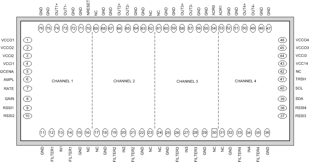
5 Pin Configuration and Functions
ONET2804TLP Bond Pad Assignment: Y Package
76-Pad Die
Top View

Bond Pad Functions
| PAD | I/O | DESCRIPTION | |
|---|---|---|---|
| NAME | NO. | ||
| ADR0 | 54 | Digital input | 2-wire interface address programming pin. Leave this pad open for a default address of 0001100. Grounding this pad changes the first address bit to a 1 (0001101). |
| ADR1 | 53 | Digital input | 2-wire interface address programming pin. Leave this pad open for a default address of 0001100. Grounding this pad changes the second address bit to a 1 (0001110). |
| AMPL | 6 | Digital input | 3-state input for amplitude control of all four channels. VCC: 500-mVPP differential output swing Open: 300-mVPP differential output swing (default) GND: 250-mVPP differential output swing |
| FILTER1 | 12, 14 | Analog output | FILTERx is the bias voltage for the photodiode cathode. These pads are biased to VCC – 100 mV. |
| FILTER2 | 19, 21 | ||
| FILTER3 | 26, 28 | ||
| FILTER4 | 33, 35 | ||
| GAIN | 8 | Digital input | 3-state input for gain control of all four channels. VCC: Minimum transimpedance Open: Default transimpedance GND: Medium transimpedance |
| GND | 11, 15, 18, 22, 25, 29, 32, 36, 47, 48, 51, 52, 55, 56, 59, 60, 63, 64, 67, 68, 71, 72, 75, 76 | Supply | Circuit ground. All GND pads are connected on the die. Bonding all pads is recommended, except for pads 11, 15, 18, 22, 25, 29, 32, and 36. |
| I2CENA | 5 | Digital input | 2-wire control option. Leave the pad unconnected for pad control of the device. Two-wire control can be enabled by applying a high signal to the pad. |
| IN1 | 13 | Analog input | INx is the data input to corresponding TIA channel (connect to photodiode anode) |
| IN2 | 20 | ||
| IN3 | 27 | ||
| IN4 | 34 | ||
| NC | 16, 17, 23, 24, 30, 31, 42, 61, 62, 69 | No connection | Do not connect |
| NRESET | 70 | Digital input | Used to reset the 2-wire state machine and registers. Leave open for normal operation and set low to reset the 2-wire interface. |
| OUT1– | 73 | Analog output | Inverted CML data output for channel x. On-chip, 50-Ω, back-terminated to VCC. |
| OUT2– | 65 | ||
| OUT3– | 57 | ||
| OUT4– | 49 | ||
| OUT1+ | 74 | Analog output | Noninverted CML data output for channel x. On-chip, 50-Ω, back-terminated to VCC. |
| OUT2+ | 66 | ||
| OUT3+ | 58 | ||
| OUT4+ | 50 | ||
| RATE | 7 | Digital input | 3-state input for bandwidth control of all four channels. VCC: Increase the bandwidth Open: 21-GHz bandwidth (default) GND: Reduce the bandwidth |
| RSSI1 | 9 | Analog output | Indicates the strength of the received signal (RSSI) for channel x if the photodiode is biased from FILTERx. The analog output current is proportional to the input data amplitude. Connect to an external resistor to ground (GND). For proper operation, ensure that the voltage at the RSSIx pad does not exceed VCC – 0.65 V. If the RSSI feature is not used, leave these pads open. |
| RSSI2 | 10 | ||
| RSSI3 | 37 | ||
| RSSI4 | 38 | ||
| SCL | 40 | Digital input | 2-wire interface serial clock input. Includes a 10-kΩ pullup resistor to VCC. |
| SDA | 39 | Digital input/output | 2-wire interface serial data input. Includes a 10-kΩ pullup resistor to VCC. |
| TRSH | 41 | Digital input | 3-state input for the threshold control. VCC: Crossing point shifted down Open: No threshold adjustment (default) GND: Crossing point shifted up |
| VCCI1 | 4 | Supply | 2.8 V to 3.47 V supply voltage for the input TIAx stage. |
| VCCI2 | 3 | ||
| VCCI3 | 44 | ||
| VCCI4 | 43 | ||
| VCCO1 | 1 | Supply | 2.8 V to 3.47 V supply voltage for the AGCx and CMLx amplifiers. |
| VCCO2 | 2 | ||
| VCCO3 | 45 | ||
| VCCO4 | 46 | ||