SNVS095F May 2004 – March 2015 LP2952-N , LP2953
PRODUCTION DATA.
- 1 Features
- 2 Applications
- 3 Description
- 4 Revision History
- 5 Pin Configuration and Functions
- 6 Specifications
- 7 Detailed Description
-
8 Application and Implementation
- 8.1 Application Information
- 8.2
Typical Applications
- 8.2.1 Basic 5-V Regulator
- 8.2.2 5-V Current Limiter with Load Fault Indicator
- 8.2.3 Low Temperature Coefficient Current Sink
- 8.2.4 5-V Regulator With Error Flags for Low Battery and Out of Regulation
- 8.2.5 5-V Battery Powered Supply With Backup and Low Battery Flag
- 8.2.6 5-V Regulator With Timed Power-On Reset
- 8.2.7 5-V Regulator With Snap-ON and Snap-OFF Features and Hysteresis
- 8.2.8 5-V Regulator With Error Flags for Low Battery and Out of Regulation With Snap-ON or Snap-OFF Output
- 8.2.9 5-V Regulator With Timed Power-On Reset, Snap-ON and Snap-OFF Features, and Hysteresis
- 9 Power Supply Recommendations
- 10Layout
- 11Device and Documentation Support
- 12Mechanical, Packaging, and Orderable Information
5 Pin Configuration and Functions
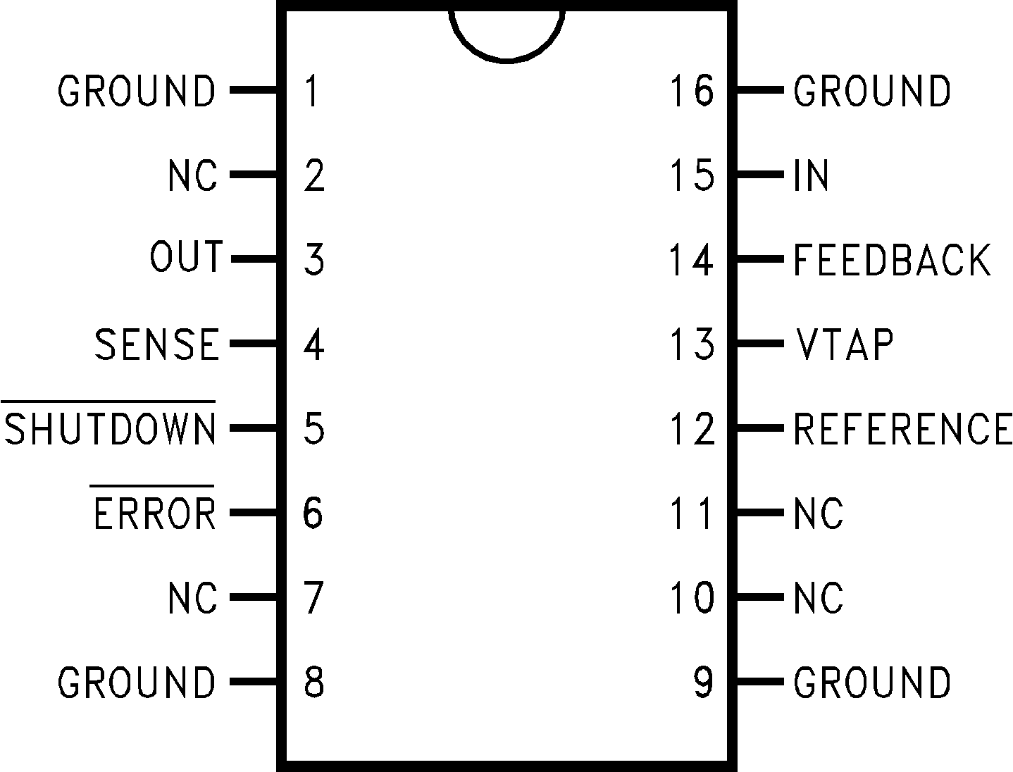
LP2952 SOIC (D) Package
16 Pins
Top View

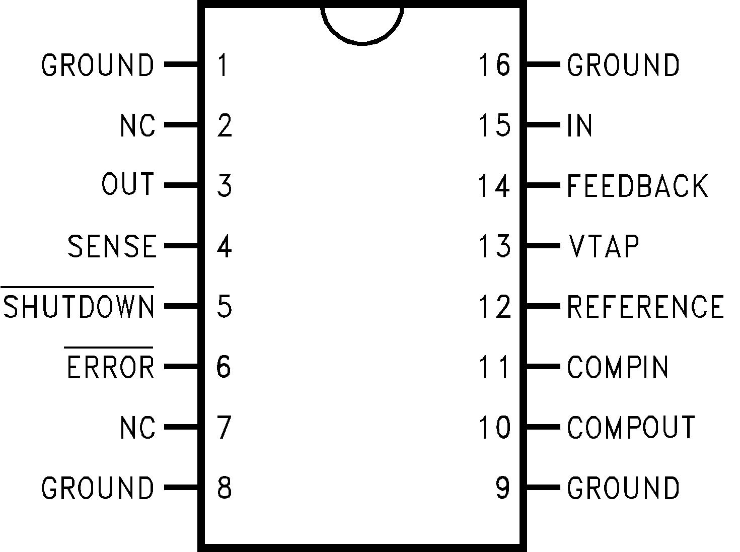
LP2953 SOIC (D) Package
16 Pins
Top View

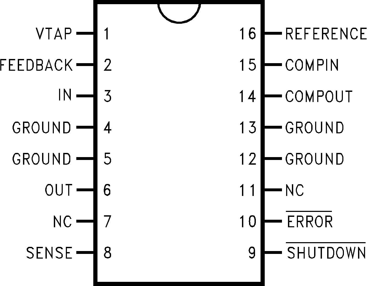
LP2953 PDIP (NBG) Package
16 Pins
Top View

Pin Functions LP2952-N
| PIN | I/O | DESCRIPTION | |
|---|---|---|---|
| NAME | SOIC(D) | ||
| ERROR | 6 | O | Error signal output |
| FEEDBACK | 14 | I | Error amplifier noninverting input |
| GROUND | 1, 8, 9, 16 | - | Ground |
| IN | 15 | I | Regulator power input |
| NC | 2, 7, 10, 11 | - | NC |
| OUT | 3 | O | Regulated output voltage |
| REFERENCE | 12 | O | Internal reference voltage output |
| SENSE | 4 | I | Feedback voltage sense input |
| SHUTDOWN | 5 | I | Shutdown input |
| VTAP | 13 | I | Internal resistor divider input |
Pin Functions LP2953
| PIN | I/O | DESCRIPTION | ||
|---|---|---|---|---|
| NAME | SOIC(D) | PDIP(NBG) | ||
| COMPIN | 10 | 15 | I | Auxiliary comparator input |
| COMPOUT | 11 | 14 | O | Auxiliary comparator output |
| ERROR | 6 | 10 | O | Error signal output |
| FEEDBACK | 14 | 2 | I | Error amplifier noninverting input |
| GROUND | 1, 8, 9, 16 | 4, 5, 12, 13 | - | Ground |
| IN | 15 | 3 | I | Regulator power input |
| NC | 2, 7 | 7, 11 | - | NC |
| OUT | 3 | 6 | O | Regulated output voltage |
| REFERENCE | 12 | 16 | O | Internal reference voltage output |
| SENSE | 4 | 8 | I | Feedback voltage sense input |
| SHUTDOWN | 5 | 9 | I | Shutdown input |
| VTAP | 13 | 1 | I | Internal resistor divider input |