SNVS764Q January 2000 – December 2017 LP2950-N , LP2951-N
PRODUCTION DATA.
- 1 Features
- 2 Applications
- 3 Description
- 4 Revision History
- 5 Voltage Options
- 6 Pin Configuration and Functions
- 7 Specifications
-
8 Detailed Description
- 8.1 Overview
- 8.2 Functional Block Diagrams
- 8.3 Feature Description
- 8.4 Device Functional Modes
-
9 Application and Implementation
- 9.1 Application Information
- 9.2
Typical Applications
- 9.2.1 1-A Regulator with 1.2-V Dropout
- 9.2.2 300-mA Regulator with 0.75-V Dropout
- 9.2.3 Wide Input Voltage Range Current Limiter
- 9.2.4 Low Drift Current Source
- 9.2.5 5-V Current Limiter
- 9.2.6 Regulator with Early Warning and Auxiliary Output
- 9.2.7 Latch Off When Error Flag Occurs
- 9.2.8 2-A Low Dropout Regulator
- 9.2.9 5-V Regulator with 2.5-V Sleep Function
- 9.2.10 Open Circuit Detector for 4 → 20-mA Current Loop
- 9.2.11 Regulator with State-of-Charge Indicator
- 9.2.12 Low Battery Disconnect
- 9.2.13 System Overtemperature Protection Circuit
- 10Power Supply Recommendations
- 11Layout
- 12Device and Documentation Support
- 13Mechanical, Packaging, and Orderable Information
封装选项
机械数据 (封装 | 引脚)
散热焊盘机械数据 (封装 | 引脚)
- DGK|8
订购信息
6 Pin Configuration and Functions
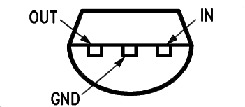
LP Package
3-Pin TO-92
Bottom View

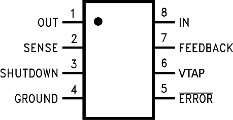
P, D, DGK Packages
8-Pin PDIP, SOIC, VSSOP
Top View

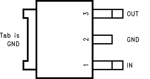
NDP Package
3-Pin TO-252
Front View

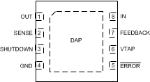
NGT Package
8-Pin WSON
Top View

Connect DAP to GND at device pin 4.
Pin Functions: LP2950-N
| PIN | I/O | DESCRIPTION | ||
|---|---|---|---|---|
| NAME | LP2950 | |||
| LP | NDP | |||
| GND | 2 | 2 | — | Ground |
| IN | 3 | 1 | I | Input supply voltage |
| OUT | 1 | 3 | O | Regulated output voltage |
Pin Functions: LP2951-N
| PIN | I/O | DESCRIPTION | ||
|---|---|---|---|---|
| NAME | LP2951 | |||
| D, DGK, P | NGT | |||
| ERROR | 5 | 5 | O | Error output |
| FEEDBACK | 7 | 7 | I | Voltage feedback input |
| GROUND | 4 | 4 | — | Ground |
| IN | 8 | 8 | I | Input supply voltage |
| OUT | 1 | 1 | O | Regulated output voltage |
| SENSE | 2 | 2 | I | Output voltage sense |
| SHUTDOWN | 3 | 3 | I | Disable device |
| VTAP | 6 | 6 | O | Internal resistor divider |