SNOS458I April 2000 – June 2016 LMV7219
PRODUCTION DATA.
7 Detailed Description
7.1 Overview
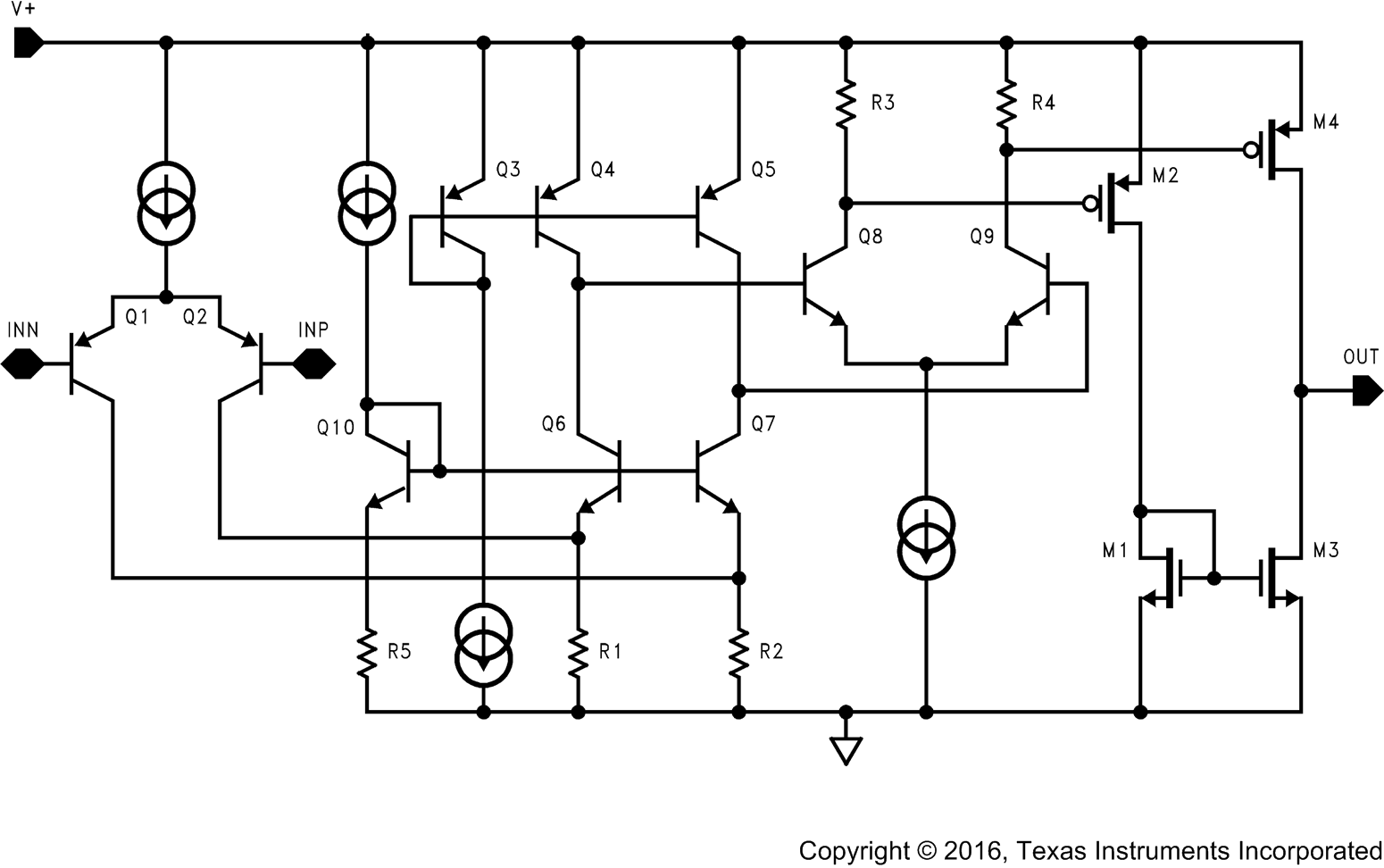
LMV7219 is a single supply comparator with internal hysteresis, 7 ns of propagation delay and only 1.1 mA of supply current.
The LMV7219 has a typical input common mode voltage range of −0.2 V below the ground to 1 V below Vcc. The differential input stage is a pair of PNP transistors, therefore, the input bias current flows out of the device. If either of the input signals falls below the negative common mode limit, the parasitic PN junction formed by the substrate and the base of the PNP will turn on, resulting in an increase of input bias current.
7.2 Functional Block Diagram

7.3 Feature Description
If one of the inputs goes above the positive common mode limit, the output will still maintain the correct logic level as long as the other input stays within the common mode range. However, the propagation delay will increase. When both inputs are outside the common mode voltage range, current saturation occurs in the input stage, and the output becomes unpredictable.
7.4 Device Functional Modes
The propagation delay does not increase significantly with large differential input voltages. However, large differential voltages greater than the supply voltage should be avoided to prevent damages to the input stage.
The LMV7219 has a push-pull output. When the output switches, there is a direct path between VCC and ground, causing high output sinking or sourcing current during the transition. After the transition, the output current decreases and the supply current settles back to about 1.1 mA at 5 V, thus conserving power consumption.
Most high-speed comparators oscillate when the voltage of one of the inputs is close to or equal to the voltage on the other input due to noise or undesirable feedback. The LMV7219 has 7 mV of internal hysteresis to counter parasitic effects and noise. The hysteresis does not change significantly with the supply voltages and the common mode input voltages as reflected in the specification table.