ZHCSCA9A March 2014 – April 2015 LMP92066
PRODUCTION DATA.
- 1 特性
- 2 应用范围
- 3 说明
- 4 简化电路原理图
- 5 修订历史记录
- 6 Pin Configuration and Functions
- 7 Specifications
-
8 Detailed Description
- 8.1 Overview
- 8.2 Functional Block Diagram
- 8.3 Features Description
- 8.4 Device Functional Modes
- 8.5
Programming
- 8.5.1 Temperature Sensor Output Data Access Registers
- 8.5.2 DAC Input Data Registers
- 8.5.3 Temperature Sensor Status Register
- 8.5.4 Override Control Register
- 8.5.5 Override Data Registers
- 8.5.6 EEPROM Control Register
- 8.5.7 Software RESET Register
- 8.5.8 Access Control Register
- 8.5.9 Block I2C Access Control Register
- 8.5.10 I2C Address LOCK Register
- 8.5.11 Output Drive Supply Status Register
- 8.5.12 Device Version Register
- 8.5.13 EEPROM Burn Counter
- 8.5.14 LUT Coefficient Registers
- 8.5.15 LUT Control Registers
- 8.5.16 Notepad Registers
- 8.6 Register Map
- 9 Application and Implementation
- 10Power Supply Recommendations
- 11Layout
- 12器件和文档支持
- 13机械、封装和可订购信息
7 Specifications
7.1 Absolute Maximum Ratings
over operating free-air temperature range (unless otherwise noted) (1)| MIN | MAX | UNIT | ||
|---|---|---|---|---|
| VDD | Supply voltage with respect to GNDA | –0.3 | 5.5 | V |
| VDDB | –0.3 | 5.5 | ||
| VIO | –0.3 | 5.5 | ||
| VSSB | –5.5 | 0.3 | ||
| GNDD | –0.3 | 0.3 | ||
| VDDB to VSSB | –0.3 | 5.5 | V | |
| Any other pins to GNDA | –0.3 | 5.5 | ||
| DAC output current | 10 | mA | ||
| Current at all other pins | 5 | |||
| Storage temperature, Tstg | –65 | 150 | °C | |
(1) Stresses beyond those listed under Absolute Maximum Ratings may cause permanent damage to the device. These are stress ratings only, which do not imply functional operation of the device at these or any other conditions beyond those indicated under Recommended Operating Conditions. Exposure to absolute-maximum-rated conditions for extended periods may affect device reliability.
7.2 ESD Ratings
| VALUE | UNIT | |||
|---|---|---|---|---|
| V(ESD) | Electrostatic discharge | Human-body model (HBM), per ANSI/ESDA/JEDEC JS-001(1) | ±2500 | V |
| Charged-device model (CDM), per JEDEC specification JESD22-C101(2) | ±1000 | |||
(1) JEDEC document JEP155 states that 500-V HBM allows safe manufacturing with a standard ESD control process.
(2) JEDEC document JEP157 states that 250-V CDM allows safe manufacturing with a standard ESD control process.
7.3 Recommended Operating Conditions
over operating free-air temperature range (unless otherwise noted)| MIN | MAX | UNIT | |||
|---|---|---|---|---|---|
| Operational temperature | –40 | 125 | °C | ||
| Specification temperature | –25 | 120 | |||
| DAC output load capacitance | 8 | 12 | µF | ||
| VDD | Supply voltage range (VDD) | 4.75 | 5.25 | V | |
| VIO | Digital I/O supply voltage | 1.65 | 3.3 | ||
| VDDB–VSSB | LDMOS mode VSSB = GNDA | 5 | |||
| GaN mode VSSB = –5 V | 5 | ||||
7.4 Thermal Information
| THERMAL METRIC(1) | PWP (HTSSOP) 16 PINS |
UNIT | |
|---|---|---|---|
| RθJA | Junction-to-ambient thermal resistance | 38.2 | °C/W |
| RθJC(top) | Junction-to-case (top) thermal resistance | 21.3 | |
| RθJB | Junction-to-board thermal resistance | 15.1 | |
| ψJT | Junction-to-top characterization parameter | 0.5 | |
| ψJB | Junction-to-board characterization parameter | 14.9 | |
| RθJC(bot) | Junction-to-case (bottom) thermal resistance | 1.4 | |
(1) For more information about traditional and new thermal metrics, see the IC Package Thermal Metrics application report, SPRA953.
7.5 Electrical Characteristics
Unless otherwise noted: VDD = 5 V ±5%, VIO = 1.8 V to 3.3 V, TA = 25°C. VDDB = 5 V ±5%, VSSB = GNDA, VDACx output range 0 V to 5 V; or VDDB = GNDA, VSSB = –5 V ±5%, VDACx output range 0 V to –5V. DAC input code range 48 to 4047. VDACX load CL = 10 µF.| PARAMETER | TEST CONDITIONS | MIN | TYP | MAX | UNIT | |
|---|---|---|---|---|---|---|
| ANALOG SIGNAL PATH CHARACTERISTICS (DAC, Buffer Amplifier, Internal Reference) | ||||||
| Resolution | –25°C < TA < 120°C | 12 | 12 | Bits | ||
| Monotonic | 12 | |||||
| DNL | Differential non-linearity | RL = 100 kΩ, –25°C < TA < 120°C | –0.99 | 1 | LSB | |
| INL | Integral non-linearity | RL = 100 kΩ, –25°C < TA < 120°C | −1.93 | 2.78 | ||
| OE | Offset error(1) | LDMOS mode, RL = 100 kΩ, –25°C < TA < 120°C |
–14 | 14 | mV | |
| LDMOS mode, RL = 100 kΩ | ±1 | |||||
| GaN mode, RL = 100 kΩ, –25°C < TA < 120°C | –16.5 | 16.5 | ||||
| OETC | Offset error temperature coefficient(1)(2) | RL = 100 kΩ, –25°C < TA < 120°C | 43 | μV/°C | ||
| GE | Gain error(1) | RL = 100 kΩ, –25°C < TA < 120°C | –0.72 | 0.74 | %FS | |
| GETC | Gain error temperature coefficient(1)(2) | RL = 100 kΩ, –25°C < TA < 120°C | 20 | ppm/°C | ||
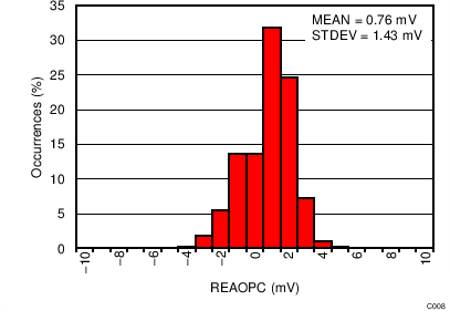
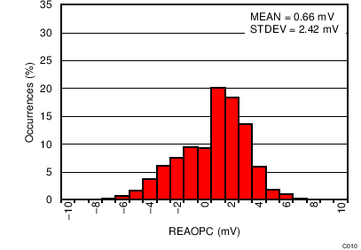
| REAOPC | Residual error after one point calibration(1)(2)(3)(4) | BASEx = 1638 (VDACX = 2 V at 24°C) –25°C < TA < 120°C |
–13.3 | 13.3 | mV | |
| BASEx = 1638 (VDACX = 2 V at 24°C) | ±2.4 | |||||
| BASEx = 819 (VDACX = 1 V at 24°C) –25°C < TA < 120°C |
–11.3 | 11.3 | ||||
| BASEx = 819 (VDACX = 1 V at 24°C) | ±2.1 | |||||
| ZCO | Zero code output (VDACx – VSSB) | LDMOS mode, RL = 100 kΩ | 0 | mV | ||
| LDMOS mode, IOUT = 10 mA | 200 | |||||
| FSO | Full-scale output at code 4095 (VDDB – VDACx) | LDMOS mode, RL = 100 kΩ | 10 | mV | ||
| LDMOS mode, IOUT = –10 mA | 150 | |||||
| IO | Continuous output current per channel allowed(5) | TA = 125°C | 10 | mA | ||
| CL | Load capacitance(5) | RL = 2 kΩ or ∞, –25°C < TA < 120°C | 12 | µF | ||
| RL = 2 kΩ or ∞ | 10 | |||||
| DAC output resistance | DACCODEx = 2048 | 3 | Ω | |||
| DAC settling time | CL = 10 µF | 250 | µs | |||
| OUTPUT SWITCH DC CHARACTERISTICS | ||||||
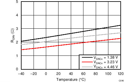
| RDRV | On Resistance of the switch between DACx and FETDRVx | –25°C < TA < 120°C | 6 | Ω | ||
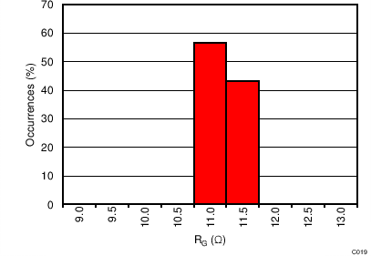
| RG | On Resistance of the switch between FETDRVx and VSSB | 11 | ||||
| TEMPERATURE SENSOR CHARACTERISTICS | ||||||
| Resolution | 0.0625 | °C/lsb | ||||
| TE | Temperature sensor error(2) | TA = –40°C to 120°C | –3.2 | 3.2 | °C | |
| Conversion time | 25 | ms | ||||
| EEPROM | ||||||
| Maximum EEPROM write cycles | 100 | |||||
| DIGITAL INPUT CHARACTERISTICS (DRVEN0, DRVEN1, SDA, and SCL) | ||||||
| VIH | Input high voltage | –25°C < TA < 120°C | 0.7 × VIO | V | ||
| VIL | Input low voltage | –25°C < TA < 120°C | 0.3 × VIO | |||
| Hysteresis | 0.2 × VIO | |||||
| CiND | Input capacitance | 5 | pF | |||
| DIGITAL INPUT CHARACTERISTICS (A0, A1) | ||||||
| VIH | Input high voltage | –25°C < TA < 120°C | 0.7 × VIO | V | ||
| VIL | Input low voltage | –25°C < TA < 120°C | 0.3 × VIO | |||
| RUP | Internal pullup resistance | 17 | kΩ | |||
| RDN | Internal pulldown resistance | 17 | ||||
| Max external capacitance(5) | 30 | pF | ||||
| DIGITAL OUTPUT CHARACTERISTICS (SDA) | ||||||
| VOL | Output low voltage | IOUT = 4 mA, –25°C < TA < 120°C | 0.4 | V | ||
| IOUT = 4 mA | 0.16 | |||||
| ILEAK | Open-drain output leakage current with output high(5) | Current from the supply rail through the pullup resistor into the drain of the open-drain output device, –25°C < TA < 120°C | ±1 | μA | ||
| COUT | Output capacitance | 4 | pF | |||
| SUPPLY CURRENT SPECIFICATIONS | ||||||
| IDD | Normal operation(6), –25°C < TA < 120°C | 2.6 | mA | |||
| While executing EEPROM BURN(7) | 4 | |||||
| While transferring EEPROM content to operating memory(8) | 9 | |||||
| IVIO | I2C inactive, –25°C < TA < 120°C | 3 | µA | |||
| I2C in fast mode, –25°C < TA < 120°C | 3.1 | |||||
| IVDDB | LDMOS mode, RL = ∞, –25°C < TA < 120°C | 1.5 | mA | |||
| IVSSB | GaN mode, RL = ∞, –25°C < TA < 120°C | –1.4 | ||||
| PWR (Conv) | Power consumption, conversion mode | All output pins RL = ∞ | 20 | mW | ||
(1) The package mechanical stress-induced parameter shift may cause the parts to manifest behavior beyond the specified limits. Mechanical stresses may also arise as a result of the PCB manufacturing process.
(2) Device specification is verified by characterization and is not tested in production.
(3) The specification is a calculated worst-case value based on the OE, OETC, GE, and GETC limits.
(4) The outcome of the REAOPC characterization of the PCB mounted devices is shown in Figure 4, Figure 5, and Figure 6 of the Typical Characteristics. The 97, randomly selected, devices from 3 diffusion lots were installed on the 4-layer RO4003 Laminate using Convection Reflow. The Look-Up-Table was set for maximum gain; for example, all DELx = 0xFF. While powered up, the devices were subjected to 3 thermal cycles, from –40°C to 125°C, during which their REAOPC was recorded.
(5) Parameter based on the process data and circuit simulation.
(6) The normal operation current through the VDD excludes the current supplied to the external load, and excludes the current required by the EPPROM BURNS and TRANSFERS.
(7) During the EEPROM BURN command execution the device activates internal systems that are not active during the Normal operation. This causes a momentary increase in supply current through the VDDpin. The duration of this temporary surge in supply current is typically 125 ms.
(8) During the data transfer from the EEPROM to the Operating memory there will be a momentary surge in supply current through the VDD pin. The duration of this surge is typically 200 µs.
7.6 Timing Requirements
Unless otherwise noted: VDD = 5 V ±5%, VIO = 1.8 V to 3.3 V. VDDB = 5 V ±5%, VSSB = GNDA; or VDDB = GNDA, VSSB = –5V ±5%.| PARAMETER | TEST CONDITIONS | MIN | MAX | UNIT | |
|---|---|---|---|---|---|
| I2C clock frequency | 10 | 400 | kHz | ||
| tLOW | Clock low time | 1.3 | µs | ||
| tHIGH | Clock high time | 0.6 | |||
| tHD-STA | Hold time repeated START condition | After this period, the first clock pulse is generated | 0.6 | ||
| tSU;STA | Setup time for a repeated START condition | 0.6 | |||
| tHD;DAT | Data hold time (Note x and y) | 0 | 900 | ns | |
| tSU;DAT | Data setup time | 100 | |||
| tf | SDA fall time | IL ≤ 3 mA and CL ≤ 400 pF | 250 | ||
| tSU;STO | Setup time for STOP condition | 0.6 | µs | ||
| tBUF | Bus free time between a STOP and START condition | 1.3 | |||
| Cb | SDA capacitive load | 400 | pF | ||
| tSP | Pulse width of spikes that must be suppressed by the input filter | 50 | ns | ||
| SCL and SDA timeout | 25 | 35 | ms | ||
7.7 Output Switching Characteristics
Unless otherwise noted: VDD = 5 V ±5%, VIO = 1.8 V to 3.3 V. VDDB = 5 V ±5%, VSSB = GNDA; or VDDB = GNDA, VSSB = –5V ±5%.| PARAMETER | TEST CONDITIONS | MIN | TYP | MAX | UNIT | |
|---|---|---|---|---|---|---|
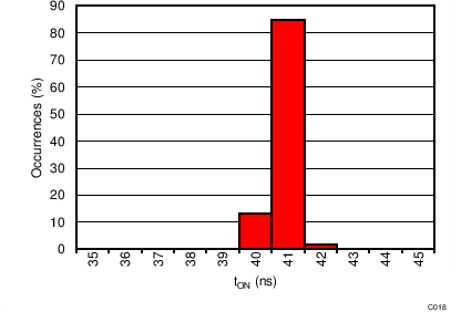
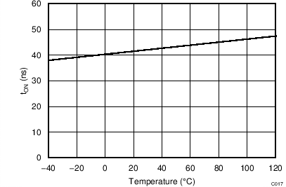
| tON | On time | DACCODEx = 4095, RL = 100 kΩ | 50 | ns | ||
| tOFF | Off time | 50 | ||||
| tBBM | Break-before-make time | 15 | ||||
| CFETDRV | FETDRV output capacitance | 10 | pF | |||
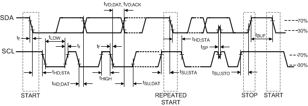 Figure 1. I2C Timing
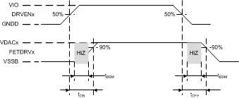 Figure 2. Switching
7.8 Typical Characteristics
Unless otherwise stated the plot data was collected under these conditions: VDD = 5 V, VDDB = 5 V, VSSB = GNDA, VIO = 3.3 V, Temperature = 24°C, RL = 100 kΩ.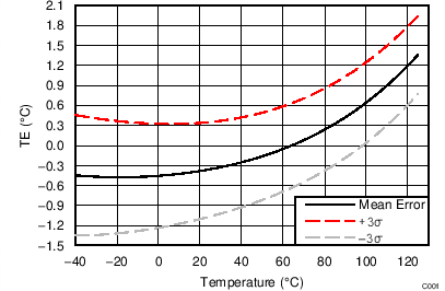
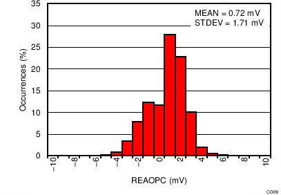
| BASE = 1638 | PCB Mounted | |
| 97 devices | 3 Cycles: –40°C to 125°C | |
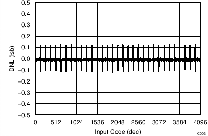
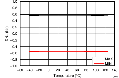
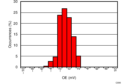
| TEMP = –40°C to 120°C | ||
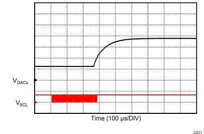
| DAC OVERRIDE MODE | I2C command triggers DAC step | |
| CL = 10 µF | Step size: 1/4 to 3/4 FS | |
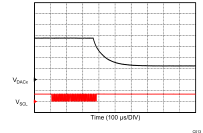
| DAC OVERRIDE MODE | I2C command triggers DAC step | |
| CL = 10 µF | Step size: 3/4 to 1/4 FS | |
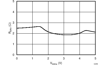
| BASE = 819 | PCB Mounted | |
| 97 devices | 3 Cycles: –40°C to 125°C | |
| BASE = 3277 | PCB Mounted | |
| 97 devices | 3 Cycles: –40°C to 125°C | |
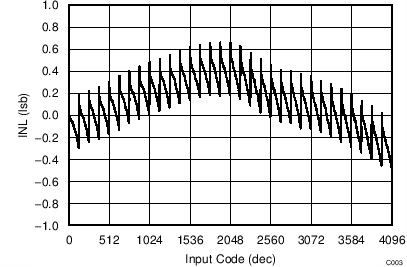
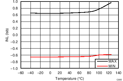
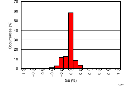
| TEMP = –40°C to 120°C | ||
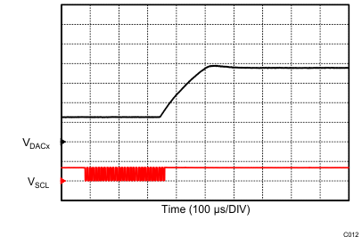
| DAC OVERRIDE MODE | I2C command triggers DAC step | |
| CL = 10 pF | Step size: 1/4 to 3/4 FS | |
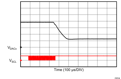
| DAC OVERRIDE MODE | I2C command triggers DAC step | |
| CL = 10 pF | Step size: 3/4 to 1/4 FS | |
