ZHCSBP0B September 2013 – March 2014 LMP91300
PRODUCTION DATA.
- 1 特性
- 2 应用范围
- 3 说明
- 4 修订历史记录
- 5 Terminal Configuration and Functions
- 6 Specifications
-
7 Detailed Description
- 7.1 Overview
- 7.2 Functional Block Diagram
- 7.3 Feature Description
- 7.4 Device Functional Modes
- 7.5 Programming
- 7.6
Register Maps
- 7.6.1 DET_H_MSB_INIT - Detection High Threshold MSB (Initial) (Address 0x66)
- 7.6.2 DET_H_LSB_INIT - Detection High Threshold LSB (Initial) (Address 0x67)
- 7.6.3 DET_L_MSB_INIT - Detection Low Threshold MSB (Initial) (Address 0x68)
- 7.6.4 DET_L_LSB_INIT - Detection Low Threshold LSB (Initial) (Address 0x69)
- 7.6.5 INFO0 - Device Information 0 (Address 0x6A)
- 7.6.6 INFO1 - Device Information 1 (Address 0x6B)
- 7.6.7 INFO2 - Device Information 2 (Address 0x6C)
- 7.6.8 INFO3 - Device Information 3 (Address 0x6D)
- 7.6.9 OSC_CONFIG_0 - Oscillator Configuration 0 Register (Address 0x6E)
- 7.6.10 45
- 7.6.11 OSC_CONFIG_1 - Oscillator Configuration 1 Register (Address 0x6F)
- 7.6.12 OSC_CONFIG_2 - Oscillator Configuration 2 Register (Address 0x70)
- 7.6.13 OSC_CONFIG_3_INIT - Oscillator Configuration 3 Register (Initial) (Address 0x71)
- 7.6.14 OUT_CONFIG_INIT - Output Configuration Register (Initial) (Address 0x72)
- 7.6.15 DET_H_MSB_FNL - Detection High Threshold MSB (Final) (Address 0x73)
- 7.6.16 DET_H_LSB_FNL - Detection High Threshold LSB (Final) (Address 0x74)
- 7.6.17 DET_L_MSB_FNL - Detection Low Threshold MSB (Final) (Address 0x75)
- 7.6.18 DET_L_LSB_FNL - Detection Low Threshold LSB (Final) (Address 0x76)
- 7.6.19 OSC_CONFIG_3_FNL - Oscillator Configuration 3 Register (Final) (Address 0x77)
- 7.6.20 OUT_CONFIG_FNL - Output Configuration Register (Final) (Address 0x78)
- 7.6.21 TEMP64 - Temperature In °C + 64 (Address 0x79)
- 7.6.22 PROXIMITY_MSB - Proximity MSB (Address 0x7A)
- 7.6.23 PROXIMITY_LSB - Proximity LSB (Address 0x7B)
- 7.6.24 STATUS - Device Status (Address 0x7E)
- 7.6.25 BURN_REQ - Burn Request (Address 0x7F)
-
8 Application and Implementation
- 8.1 Application Information
- 8.2
Typical Application
- 8.2.1 Design Requirements
- 8.2.2
Detailed Design Procedure
- 8.2.2.1 Quick Start
- 8.2.2.2 Determining The RP of an LC Tank
- 8.2.2.3 Component Selection And Layout
- 8.2.2.4 CF (CFA and CFB Terminals)
- 8.2.2.5 NTC (TEMP+ Terminal)
- 8.2.2.6 C1
- 8.2.2.7 CV+/EXT E
- 8.2.2.8 CBY (CBY Terminal)
- 8.2.2.9 RSENSE
- 8.2.2.10 REXT B (EXT B Terminal):
- 8.2.2.11 R1
- 8.2.2.12 SENSE1+ And SENSE2+ Terminals (RSENSE1+, RSENSE2+)
- 8.2.2.13 NPN
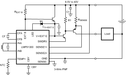
- 8.2.2.14 PNP
- 8.2.2.15 LED
- 8.2.2.16 LC Tank and INA and INB Terminals
- 8.2.2.17 SWDRV Terminal
- 8.2.2.18 P1 To P5 Terminals
- 8.2.2.19 GND Terminals
- 8.2.2.20 NC Terminals
- 8.2.2.21 Exposed DAP
- 8.2.2.22 SENSE-
- 8.2.3 Look-Up Table Calibration
- 9 Power Supply Recommendations
- 10Layout
- 11器件和文档支持
- 12机械封装和可订购信息
1 特性
2 应用范围
- 工业用近距离检测
- 工业用生产线
- 工业自动化
3 说明
LMP91300 是一款针对工业用感应式近距离传感器中的使用而进行优化的完整模拟前端 (AFE)。 LMP91300 直接将外部 LC 谐振回路的 RP 转换为一个数字值。
完全支持后置制造配置和校准。 使用一个外部温度传感器对传感器的温度相关性进行数字化补偿。 LMP91300 提供可编程阀值、可编程温度补偿和可编程振荡频率范围。 由于其可编程性,LMP91300 可与多种外部电感器一同使用,并且其检测阀值可被调节至所需的检测距离。
一个内部电压稳压器可使器件由 6.5V 至 40V 的电源供电运行。 输出可被设定为驱动一个 NPN 或 PNP 模式的外部晶体管。
采用 4mm x 5mm 24 端子超薄四方扁平无引线 (WQFN) 和 2.05mm x 2.67mm 20 端子 DSBGA 封装,LMP91300 的运行温度范围为 -40°C 至 +125°C。
器件信息
| 订货编号 | 封装 | 封装尺寸 |
|---|---|---|
| LMP91300NHZ | WQFN (24) | 4mm x 5mm |
| LMP91300YZR | DSBGA (20) | 2.05mm x 2.67mm |