SNOSAW6E January 2008 – December 2014 LMP7721
PRODUCTION DATA.
- 1 Features
- 2 Applications
- 3 Description
- 4 Revision History
- 5 Pin Configuration and Functions
- 6 Specifications
- 7 Detailed Description
- 8 Application and Implementation
- 9 Power Supply Recommendations
- 10Layout
- 11Device and Documentation Support
- 12Mechanical, Packaging, and Orderable Information
8 Application and Implementation
NOTE
Information in the following applications sections is not part of the TI component specification, and TI does not warrant its accuracy or completeness. TI’s customers are responsible for determining suitability of components for their purposes. Customers should validate and test their design implementation to confirm system functionality.
8.1 Application Information
The LMP7721 is specified for operation from 1.8 V to 5.5 V. Many of the specifications apply from –40°C to 125°C. Parameters that can exhibit significant variance with regard to operating voltage or temperature are presented in the Typical Characteristics section.
8.1.1 Using a Guard
In order to take full advantage of the LMP7721’s ultra-low input bias current, a "Guard" trace is recommended when designing sub-nanoamp systems.
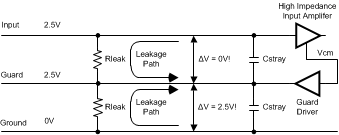 Figure 46. Guarding Theory
A "Guard" is a driven trace or shield that physically surrounds the input trace and feedback circuitry that is held at a potential equal to the average input signal potential. Since the input circuitry and the guard are kept at the same potential, the leakage current between the two nodes is practically zero. The guard is a low-impedance node, so any external leakages will "leak" into the guard and not into the protected input. One benefit of using a guard is it cancels the effect of the added stray and cable capacitance at low frequencies (but cannot cancel the sensor or amplifier input capacitance).
The guard potential may be taken from the inverting input (summing node) in noninverting and buffer applications. An example of this is shown in Figure 47 If the guarding needs to extend beyond the immediate local area around the IC, then a buffer should be used to drive the guard to prevent adding additional capacitance to the inverting node.
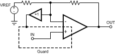 Figure 47. Guarding the Noninverting Configuration
The guard potential may be taken from the noninverting input or reference voltage in inverting or transimpedance applications. An example of this is shown in Figure 48
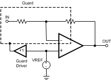 Figure 48. Guarding the Inverting or Transimpedance Configuration
The gain of the buffer should be slightly less than one to prevent oscillations and should be current limited to protect against short circuits. The buffer amplifier should also be capable of driving large capacitive loads. To satisfy these two requirements, a small series output resistor is usually placed on the buffer output in the range of 100 Ω to 1 kΩ.
For optimum results, the guard should completely enclose the input circuitry within a conductive "cocoon", including above and below the circuitry. A cover or shield connected to the guard should protect the circuitry above (or below) the PC board. Do not forget about thru-hole devices (like leaded photodiodes or connectors) that may expose high-impedance nodes to the opposite side of the board.
The guard trace should not be relied upon as the only method of shielding. A ground plane or shield should surround and protect the guard from large external leakages and noise, as the guard trace has the potential to couple noise back into the input. For more information on guarding, please see the articles referenced in Related Documentation.
8.1.2 Use Triaxial Cable
A triaxial cable or connector is similar to a coaxial cable or connector and is often referred to as “triax”. The triaxial cable extends the guard protection through the length of the cable by adding a second internal guard "shield" around the center conductor in addition to the outer ground shield. Figure 49 shows the structure of the triax connector.
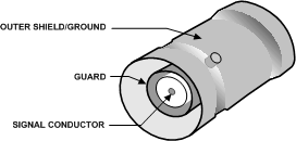 Figure 49. The Structure of a Triax
8.1.3 Properly Clean the Assembly
Proper cleaning of the board is very critical to providing the expected sub-picoamp performance. Properly cleaning the board and components takes a few extra steps over conventional board cleaning methods. Leftover flux residue, moisture and cleaning solvent residues will severely degrade the low-current performance.
If using "water soluble" or "no clean" flux, a second cleaning step is needed. These fluxes still leave a film behind that can attract contaminates and dust. The board should be washed with fresh isopropyl alcohol or methanol and baked to make sure all remaining traces of moisture are removed from the board. Areas between the component leads should be scrubbed and areas under surface mount devices thoroughly flushed. The board should be re-cleaned after any rework to components within the guarded areas. Boards should be handled by the edges and stored in sealed containers with desiccant.
8.2 Typical Application
The following application examples highlight only a few of the circuits where the LMP7721 can be used.
A CMOS input stage with ultra-low input bias current, negligible input current noise, and low input voltage noise allows the LMP7721 to provide high fidelity amplification. In addition, the LMP7721 has a 17 MHz gain bandwidth product, which enables high gain at wide bandwidth. A rail-to-rail output swing at 5.5-V power supply allows detection and amplification of a wide range of input currents. These properties make the LMP7721 ideal for transimpedance amplification.
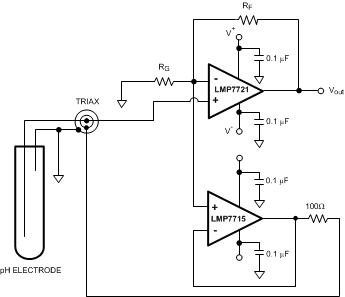 Figure 50. LMP7721 as pH Electrode Amplifier
8.2.1 Design Requirements
The output of a pH electrode is typically 59.16 mV per pH unit at 25°C, for an output range of 414 mV to −414 mV as the pH changes from 0 to 14 at 25°C.
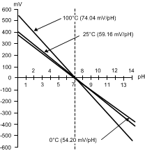 Figure 51. pH Electrode Transfer Function
The output impedance of a pH electrode is extremely high, ranging from 10 MΩ to 1000 MΩ. The ultra low input bias current of the LMP7721 allows the voltage error produced by the input bias current and electrode resistance to be minimal. For example, the output impedance of the pH electrode used is 10 MΩ, if an op amp with 3 nA of Ibias is used, the error caused due to this amplifier’s input bias current and the source resistance of the pH electrode is 30 mV! This error can be greatly reduced to 30 nV by using the LMP7721.
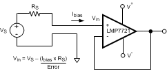 Figure 52. Error Caused by Amplifier’s Input Bias Current and Sensor Source Impedance
8.2.2 Detailed Design Procedure
The output voltage of the pH electrode will range from 54.2 mV/pH at 0°C, to 74.04 mV/pH at 100°C. The maximum input voltage will then be ±74.04 mV * 7 = ±518.3 mV. Allowing for output swing and offset headroom, the maximum output swing should be limited to ±2.4V. The amplifier gain would then be 2.4 V / 0.5183 V = 4.6 V/V.
With RF = 3.57 kΩ and RG = 1 kΩ, the gain would be 4.57 V/V.
The output voltage from the pH electrode is fed to the signal conductor of the triax and then sent to the non-inverting input of the LMP7721. In this application, the inverting input is a low impedance node and hence is used to drive the LMP7715 which acts as a guard driver. The output of the guard driver is connected to the guard of the triax through a 100-Ω isolation resistor.
Figure 50 is an example of the LMP7721 used as a pH sensor amplifier.
8.2.3 Application Curve
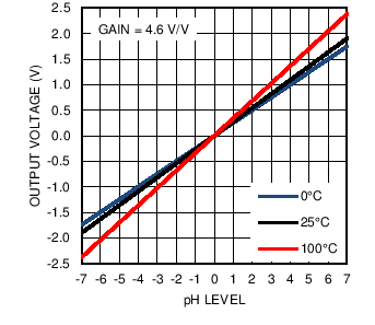 Figure 53. Output Voltage vs. pH Level