SNOSB18I April 2010 – December 2014 LMH6629
PRODUCTION DATA.
- 1 Features
- 2 Applications
- 3 Description
- 4 Revision History
- 5 Pin Configuration and Functions
- 6 Specifications
-
7 Detailed Description
- 7.1 Overview
- 7.2 Functional Block Diagram
- 7.3
Feature Description
- 7.3.1 WSON-8 Control Pins and SOT-23-5 Comparison
- 7.3.2 Compensation
- 7.3.3 Cancellation of Offset Errors Due to Input Bias Currents
- 7.3.4 Total Input Noise vs. Source Resistance
- 7.3.5 Noise Figure
- 7.3.6 Single-Supply Operation
- 7.3.7 Low-Noise Transimpedance Amplifier
- 7.3.8 Low-Noise Integrator
- 7.3.9 High-Gain Sallen-Key Active Filters
- 7.4 Device Functional Modes
- 8 Application and Implementation
- 9 Power Supply Recommendations
- 10Layout
- 11Device and Documentation Support
- 12Mechanical, Packaging, and Orderable Information
6 Specifications
6.1 Absolute Maximum Ratings
over operating free-air temperature range (unless otherwise noted) (1)(2)(3)| MIN | MAX | UNIT | ||
|---|---|---|---|---|
| Positive Supply Voltage | −0.5 | 6.0 | V | |
| Differential Input Voltage | 3 | V | ||
| Input current | ±10 | mA | ||
| Analog Input Voltage | −0.5 to VS | V | ||
| Digital Input Voltage | −0.5 to VS | V | ||
| Junction Temperature | +150 | °C | ||
| Storage Temperature (Tstg) | −65 | +150 | °C | |
(1) Stresses beyond those listed under Absolute Maximum Ratings may cause permanent damage to the device. These are stress ratings only, which do not imply functional operation of the device at these or any other conditions beyond those indicated under Recommended Operating Conditions. Exposure to absolute-maximum-rated conditions for extended periods may affect device reliability.
(2) If Military/Aerospace specified devices are required, please contact the Texas Instruments Sales Office/ Distributors for availability and specifications.
(3) Electrical table values apply only for factory testing conditions at the temperature indicated. Factory testing conditions result in very limited self-heating of the device such that TJ = TA. No guarantee of parametric performance is indicated in the electrical tables under conditions of internal self-heating where TJ > TA.
6.2 ESD Ratings
| VALUE | UNIT | |||
|---|---|---|---|---|
| V(ESD) | Electrostatic discharge | Human-body model (HBM), per ANSI/ESDA/JEDEC JS-001(1) | ±2000 | V |
| Machine model | ±200 | |||
| Charged-device model (CDM), per JEDEC specification JESD22-C101(2) | ±750 | |||
(1) JEDEC document JEP155 states that 500-V HBM allows safe manufacturing with a standard ESD control process. Manufacturing with less than 500-V HBM is possible with the necessary precautions. Pins listed as ±2000 V may actually have higher performance.
(2) JEDEC document JEP157 states that 250-V CDM allows safe manufacturing with a standard ESD control process. Manufacturing with less than 250-V CDM is possible with the necessary precautions. Pins listed as ±750 V may actually have higher performance.
6.3 Recommended Operating Conditions
over operating free-air temperature range (unless otherwise noted) (1)| MIN | NOM | MAX | UNIT | ||
|---|---|---|---|---|---|
| Supply Voltage (V+ - V−) | 2.7 | 5.5 | V | ||
| Operating Temperature Range | −40 | +125 | °C | ||
6.4 Thermal Information
| THERMAL METRIC(1) | DBV | NGQ08A | UNIT | |
|---|---|---|---|---|
| 5 PINS | 8 PINS | |||
| RθJA | Junction-to-ambient thermal resistance | 179 | 71 | °C/W |
(1) For more information about traditional and new thermal metrics, see the IC Package Thermal Metrics application report, SPRA953.
6.5 Electrical Characteristics 5V
The following specifications apply for single supply with VS = 5 V, RL = 100 Ω terminated to 2.5 V, gain = 10V/V, VO = 2VPP, VCM = VS/2, COMP Pin = HI (WSON-8 package), unless otherwise noted.(2)| PARAMETER | TEST CONDITIONS | TA = 25°C | UNIT | ||||
|---|---|---|---|---|---|---|---|
| MIN(2) | TYP(3) | MAX(2) | |||||
| DYNAMIC PERFORMANCE | |||||||
| SSBW | Small Signal −3dB bandwidth | VO = 200 mVPP, WSON-8 package | 900 | MHz | |||
| VO = 200 mVPP, SOT-23-5 package | 1000 | ||||||
| AV= 4, VO = 200 mVPP, COMP Pin = LO |
800 | ||||||
| LSBW | Large signal −3dB bandwidth | VO = 2VPP | 380 | MHz | |||
| COMP Pin = LO, AV= 4, VO = 2VPP | 190 | ||||||
| 0.1 dB bandwidth | AV= 10, VO = 200 mVPP, WSON-8 package | 330 | MHz | ||||
| AV= 10, VO = 200 mVPP, SOT-23-5 package | 190 | ||||||
| AV= 4, VO = 200 mVPP, COMP Pin = LO |
95 | ||||||
| Peaking | VO = 200 mVPP, WSON-8 package | 0 | dB | ||||
| VO = 200 mVPP, SOT-23-5 package | 2 | ||||||
| SR | Slew rate | AV= 10, 2 V step | 1600 | V/μs | |||
| AV= 4, 2 V step, COMP Pin = LO | 530 | ||||||
| tr/ tf | Rise/fall time | AV= 10, 2 V step, 10% to 90%, WSON-8 package |
0.90 | ns | |||
| AV= 10, 2 V step, 10% to 90%, SOT-23-5 package |
0.95 | ||||||
| AV= 4, 2 V step, 10% to 90%, COMP Pin = LO, (Slew Rate Limited) |
2.8 | ||||||
| Ts | Settling time | AV= 10, 1 V step, ±0.1% | 42 | ||||
| Overload recovery | VIN = 1 VPP | 2 | |||||
| NOISE and DISTORTION | |||||||
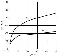
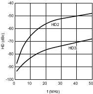
| HD2 | 2nd Order distortion | fc = 1 MHz, VO = 2 VPP | −90 | dBc | |||
| COMP Pin = LO, AV= 4, fc = 1 MHz, VO = 2 VPP |
−88 | ||||||
| fc = 10 MHz, VO = 2 VPP | −70 | ||||||
| COMP Pin = LO, fc = 10 MHz, AV= 4 V, VO = 2 VPP |
−65 | ||||||
| HD3 | 3rd Order distortion | fc = 1 MHz, VO = 2VPP | −94 | dBc | |||
| COMP Pin = LO, AV= 4, fc = 1 MHz, VO = 2 VPP |
−87 | ||||||
| fc = 10 MHz, VO = 2 VPP | −82 | ||||||
| COMP Pin = LO, fc = 10 MHz, VO = 2VPP | −75 | ||||||
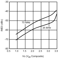
| OIP3 | Two-tone 3rd order intercept point | fc = 25 MHz, VO = 2 VPP composite | 31 | dBm | |||
| fc = 75 MHz, VO = 2 VPP composite | 27 | ||||||
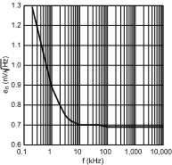
| en | Noise voltage | Input referred f > 1MHz | 0.69 | nV/√Hz | |||
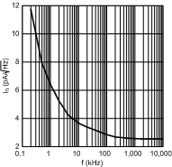
| in | Noise current | 2.6 | pA/√Hz | ||||
| NF | Noise figure | RS = RT = 50 Ω | 8.0 | dB | |||
| ANALOG I/O | |||||||
| CMVR | Input voltage range | CMRR > 70 dB, WSON-8 package | −0.30 | 3.8 | V | ||
| CMRR > 70 dB, SOT-23-5 package | −0.30 to 3.8 | ||||||
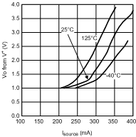
| VO | Output voltage range | RL = 100 Ω to VS/2 | 0.89 | 0.82 to 4.19 | 4.0 | V | |
| -40°C ≤ TJ ≤ +125°C | 0.95 | 3.9 | |||||
| No Load | 0.76 | 0.72 to 4.28 | 4.1 | ||||
| -40°C ≤ TJ ≤ +125°C | 0.85 | 4.0 | |||||
| IOUT | Linear output current | VO = 2.5 V (1) | 250 | mA | |||
| VOS | Input offset voltage | ±150 | ±780 | µV | |||
| -40°C ≤ TJ ≤ +125°C | ±800 | ||||||
| TcVOS | Input offset voltage temperature drift | See (4) | ±0.45 | μV/°C | |||
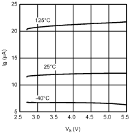
| IBI | Input bias current | See (5) | −15 | −23 | μA | ||
| -40°C ≤ TJ ≤ +125°C | −37 | ||||||
| IOS | Input offset current | ±0.1 | ±1.8 | μA | |||
| -40°C ≤ TJ ≤ +125°C | ±3.0 | ||||||
| TCIOS | Input offset voltage temperature drift | See (4) | ±2.8 | nA/°C | |||
| CCM | Input capacitance | Common Mode | 1.7 | pF | |||
| CDIFF | Differential Mode(6) | 4 | |||||
| RCM | Input resistance | Common Mode | 450 | kΩ | |||
| MISCELLANEOUS PARAMETERS | |||||||
| CMRR | Common mode rejection ratio | VCM from 0 V to 3.7 V, WSON-8 package | 82 | 87 | dB | ||
| -40°C ≤ TJ ≤ +125°C | 70 | ||||||
| VCM from 0 V to 3.7 V, SOT-23-5 package | 87 | ||||||
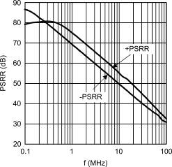
| PSRR | Power supply rejection ratio | 81 | 83 | ||||
| -40°C ≤ TJ ≤ +125°C | 78 | ||||||
| AVOL | Open loop gain | WSON-8 package | 74 | 78 | |||
| -40°C ≤ TJ ≤ +125°C | 72 | ||||||
| SOT-23-5 package | 78 | ||||||
| DIGITAL INPUTS/TIMING | |||||||
| VIL | Logic low-voltage threshold | PD and COMP pins, WSON-8 package | 0.8 | V | |||
| VIH | Logic high-voltage threshold | PD and COMP pins, WSON-8 package | 2.5 | ||||
| IIL | Logic Low-bias current | PD and COMP pins = 0.8 V, WSON-8 package(5) | −23 | −28 | −34 | µA | |
| -40°C ≤ TJ ≤ +125°C | −19 | −38 | |||||
| IIH | Logic High-bias current | PD and COMP pins = 2.5 V, WSON-8 package(5) | −16 | −22 | −27 | ||
| -40°C ≤ TJ ≤ +125°C | −14 | −29 | |||||
| Ten | Enable time | WSON-8 package | 75 | ns | |||
| Tdis | Disable time | 80 | |||||
| POWER REQUIREMENTS | |||||||
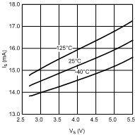
| IS | Supply current | No Load, Normal Operation (PD Pin = HI or open for WSON-8 package) | 15.5 | 16.7 | mA | ||
| -40°C ≤ TJ ≤ +125°C | 18.2 | ||||||
| No Load, Shutdown (PD Pin =LO for WSON-8 package) | 1.1 | 1.85 | |||||
| -40°C ≤ TJ ≤ +125°C | 2.0 | ||||||
(1) The maximum continuous output current (IOUT) is determined by device power dissipation limitations. Continuous short circuit operation at elevated ambient temperature can result in exceeding the maximum allowed junction temperature of 150°C
(2) All limits are ensured by testing or statistical analysis
(3) Typical numbers are the most likely parametric norm.
(4) Drift determined by dividing the change in parameter at temperature extremes by the total temperature change.
(5) Negative input current implies current flowing out of the device
(6) Simulation results.
6.6 Electrical Characteristics 3.3V
The following specifications apply for single supply with VS = 3.3 V, RL = 100 Ω terminated to 1.65 V, gain = 10V/V, VO = 1 VPP, VCM = VS/2, COMP Pin = HI (WSON-8 package), unless otherwise noted.(2)| PARAMETER | TEST CONDITIONS | TA = 25°C | UNIT | ||||
|---|---|---|---|---|---|---|---|
| MIN(4) | TYP(5) | MAX(4) | |||||
| DYNAMIC PERFORMANCE | |||||||
| SSBW | Small signal −3dB bandwidth | VO = 200 mVPP, WSON-8 package | 820 | MHz | |||
| VO = 200 mVPP, SOT-23-5 package | 950 | ||||||
| COMP Pin = LO, AV= 4, VO = 200 mVPP |
730 | ||||||
| LSBW | Large signal −3dB bandwidth | VO = 1VPP | 540 | MHz | |||
| COMP Pin = LO, AV= 4, VO = 1VPP | 320 | ||||||
| 0.1 dB Bandwidth | AV= 10, VO = 200 mVPP, WSON-8 package |
330 | MHz | ||||
| AV= 10, VO = 200 mVPP, SOT-23-5 package |
190 | ||||||
| COMP Pin = LO, AV= 4, VO = 200 mVPP |
85 | ||||||
| Peaking | VO = 200 mVPP, WSON-8 package | 0 | dB | ||||
| VO = 200 mVPP, SOT-23-5 package | 1.8 | ||||||
| SR | Slew rate | AV= 10, 1.3V step | 1100 | V/µs | |||
| COMP Pin = LO, AV= 4, 1.3V step | 500 | ||||||
| tr/ tf | Rise/fall time | AV= 10, 1V step, 10% to 90%, WSON-8 package |
0.7 | ns | |||
| AV= 10, 1V step, 10% to 90%, SOT-23-5 package |
0.55 | ||||||
| AV= 4, COMP Pin = LO, 1V step, 10% to 90% (Slew Rate Limited) | 1.3 | ||||||
| Ts | Settling time | AV= 10, 1V step, ±0.1% | 70 | ||||
| Overload recovery | VIN = 1VPP | 2 | |||||
| NOISE and DISTORTION | |||||||
| HD2 | 2nd Order distortion | fc = 1MHz, VO = 1VPP | -82 | dBc | |||
| COMP Pin = LO, AV= 4, fc = 1MHz, VO = 1VPP |
-88 | ||||||
| fc = 10 MHz, VO = 1VPP | -67 | ||||||
| COMP Pin = LO, fc = 10 MHz, AV= 4V, VO = 1VPP |
-74 | ||||||
| HD3 | 3rd Order distortion | fc = 1MHz, VO = 1VPP | -94 | dBc | |||
| COMP Pin = LO, AV= 4, fc = 1MHz, VO = 1VPP |
-112 | ||||||
| fc = 10 MHz, VO = 1VPP | -79 | ||||||
| COMP pin = LO, fc = 10 MHz, VO = 1VPP |
-96 | ||||||
| OIP3 | Two-tone 3rd order intercept point | fc = 25 MHz, VO = 1VPP composite | 30 | dBm | |||
| fc = 75 MHz, VO = 1VPP composite | 26 | ||||||
| en | Noise voltage | Input referred, f > 1MHz | 0.69 | nV/√Hz | |||
| in | Noise current | 2.6 | pA/√Hz | ||||
| NF | Noise figure | RS = RT = 50 Ω | 8.0 | dB | |||
| ANALOG I/O | |||||||
| CMVR | Input voltage range | CMRR > 70 dB, WSON-8 package | -0.30 | 2.1 | V | ||
| CMRR > 70 dB, SOT-23-5 package | -0.30 to 2.1 | ||||||
| VO | Output voltage range | RL = 100 Ω to VS/2 | 0.90 | 0.79 to 2.50 | 2.4 | ||
| -40°C ≤ TJ ≤ +125°C | 0.95 | 2.3 | |||||
| No load | 0.76 | 0.70 to 2.60 | 2.5 | ||||
| -40°C ≤ TJ ≤ +125°C | 0.80 | 2.4 | |||||
| IOUT | Linear output current | VO = 1.65 V(3) | 230 | mA | |||
| VOS | Input offset voltage | ±150 | ±680 | µV | |||
| -40°C ≤ TJ ≤ +125°C | ±700 | ||||||
| TcVOS | Input offset voltage temperature drift | See (6) | ±1 | µV/°C | |||
| IBI | Input bias current | See (7) | -15 | -23 | µA | ||
| -40°C ≤ TJ ≤ +125°C | -35 | ||||||
| IOS | Input offset current | ±0.13 | ±1.8 | ||||
| -40°C ≤ TJ ≤ +125°C | ±3.0 | ||||||
| TCIOS | Input offset voltage temperature drift | See (6) | ±3.2 | nA/°C | |||
| CCM | Input capacitance | Common Mode | 1.7 | pF | |||
| CDIFF | Differential Mode(8) | 4 | |||||
| RCM | Input resistance | Common Mode | 1 | MΩ | |||
| MISCELLANEOUS PARAMETERS | |||||||
| CMRR | Common mode rejection ratio | VCM from 0 V to 2.0 V, WSON-8 package | 84 | 87 | dB | ||
| -40°C ≤ TJ ≤ +125°C | 81 | ||||||
| VCM from 0 V to 2.0 V, SOT-23-5 package |
87 | ||||||
| PSRR | Power supply rejection ratio | 82 | 84 | ||||
| -40°C ≤ TJ ≤ +125°C | 79 | ||||||
| AVOL | Open loop gain | WSON-8 package | 78 | 79 | |||
| -40°C ≤ TJ ≤ +125°C | 73 | ||||||
| SOT-23-5 package | 79 | ||||||
| DIGITAL INPUTS/TIMING | |||||||
| VIL | Logic low-voltage threshold | PD and COMP pins, WSON-8 package | 0.8 | V | |||
| VIH | Logic high-voltage threshold | 2.0 | |||||
| IIL | Logic low-bias current | PD and COMP pins = 0.8 V, WSON-8 package(7) |
-17 | -23 | -28 | µA | |
| -40°C ≤ TJ ≤ +125°C | -14 | -32 | |||||
| IIH | Logic high-bias current | PD and COMP pins = 2.0 V, WSON-8 package(7) | -16 | -22 | -27 | ||
| -40°C ≤ TJ ≤ +125°C | -13 | -31 | |||||
| Ten | Enable time | WSON-8 package | 75 | ns | |||
| Tdis | Disable time | 80 | |||||
| POWER REQUIREMENTS | |||||||
| IS | Supply current | No Load, Normal Operation (PD Pin = HI or open for WSON-8 package) | 13.7 | 14.9 | mA | ||
| -40°C ≤ TJ ≤ +125°C | 16.0 | ||||||
| No Load, Shutdown (PD Pin = LO for WSON-8 package) | 0.89 | 1.4 | |||||
| -40°C ≤ TJ ≤ +125°C | 1.5 | ||||||
(1) Absolute maximum ratings indicate limits beyond which damage to the device may occur. Operating Ratings indicate conditions for which the device is intended to be functional, but specific performance is not ensured. For ensured specifications and the test conditions, see the Electrical Characteristics.
(2) Electrical table values apply only for factory testing conditions at the temperature indicated. Factory testing conditions result in very limited self-heating of the device such that TJ = TA. No guarantee of parametric performance is indicated in the electrical tables under conditions of internal self-heating where TJ > TA.
(3) The maximum continuous output current (IOUT) is determined by device power dissipation limitations. Continuous short circuit operation at elevated ambient temperature can result in exceeding the maximum allowed junction temperature of 150°C
(4) All limits are ensured by testing or statistical analysis.
(5) Typical numbers are the most likely parametric norm.
(6) Drift determined by dividing the change in parameter at temperature extremes by the total temperature change.
(7) Negative input current implies current flowing out of the device.
(8) Simulation results.
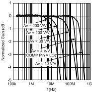
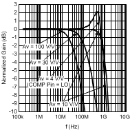
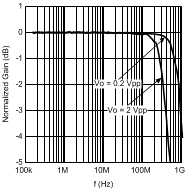
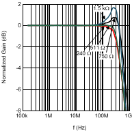
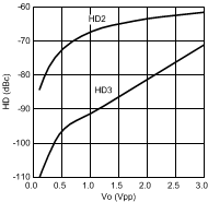
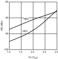
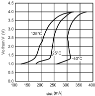
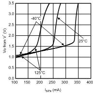
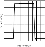
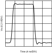
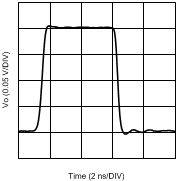
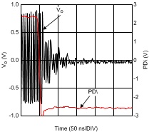
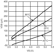
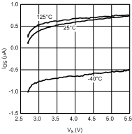
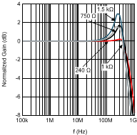
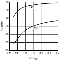
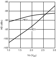
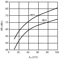
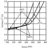
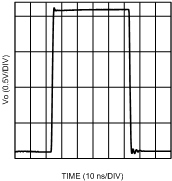
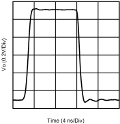
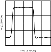
6.7 Typical Performance Characteristics
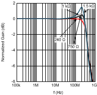
Unless otherwise specified, VS = ±2.5V, Rf = 240 Ω, RL = 100 Ω, VO = 2 VPP, COMP pin = HI, AV = +10 V/V, WSON-8 and SOT-23-5 packages (unless specifically noted).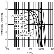
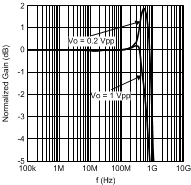
| Vo = 2 Vpp | ||
| Vo = 2 Vpp | ||
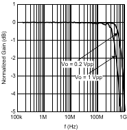
| Vo = 0.2 Vpp | ||
WSON-8 Package
| Av = 10 V/V | ||
with Varying VO, WSON-8 Package
| Av = 10 V/V | Vs = +/-1.5 V | |
with Varying VO, WSON-8 Package
| Av = 4 V/V | COMP Pin = LO | |
with Varying VO, WSON-8 Package
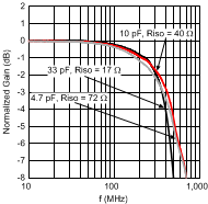
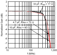
| RL = 100 Ω || CL | ||
| RISO as noted (measured @ CL) | ||
| VS = ±1.5 V | VO = 1 VPP | |
| 20 MHz | ||
| 1 MHz | ||
| 1 MHz | Vout = 2 Vpp | |
| Vo = 2 Vpp | ||
vs. Output Voltage
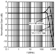
| AV= 4V/V | COMP Pin = LO | |
| Vs = 3.3 V | ||
| Vs = 3.3 V | ||
(Typical Unit)
| Vo = 1 Vpp | Vs = ±1.5V | |
| Vo = 1 Vpp | Vs = ±1.5 V | |
| Vo = 0.2 Vpp | ||
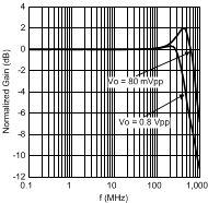
SOT-23-5 Package
| Av=10 V/V | ||
with Varying VO, SOT-23-5 Package
| Av=10 V/V | Vs= +/-1.5 V | |
with Varying VO, SOT-23-5 Package
| Av = 4 V/V | Vs = ±1.5 V | COMP Pin = LO |
with Varying VO, WSON-8 Package
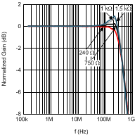
| RL = 100 Ω || CL, AV = 4 V/V | ||
| COMP Pin = LO | ||
| RISO as noted (measured @ CL) | ||
WSON-8 Package
| VS = ± 1.5 V | VO = 1 VPP | |
| 20 MHz | ||
| 1 MHz | ||
| 1 MHz | Vout = 2 Vpp | |
| Vo = 2 Vpp | ||
(Typical Unit)