SNOSB18I April 2010 – December 2014 LMH6629
PRODUCTION DATA.
- 1 Features
- 2 Applications
- 3 Description
- 4 Revision History
- 5 Pin Configuration and Functions
- 6 Specifications
-
7 Detailed Description
- 7.1 Overview
- 7.2 Functional Block Diagram
- 7.3
Feature Description
- 7.3.1 WSON-8 Control Pins and SOT-23-5 Comparison
- 7.3.2 Compensation
- 7.3.3 Cancellation of Offset Errors Due to Input Bias Currents
- 7.3.4 Total Input Noise vs. Source Resistance
- 7.3.5 Noise Figure
- 7.3.6 Single-Supply Operation
- 7.3.7 Low-Noise Transimpedance Amplifier
- 7.3.8 Low-Noise Integrator
- 7.3.9 High-Gain Sallen-Key Active Filters
- 7.4 Device Functional Modes
- 8 Application and Implementation
- 9 Power Supply Recommendations
- 10Layout
- 11Device and Documentation Support
- 12Mechanical, Packaging, and Orderable Information
10 Layout
10.1 Layout Guidelines
Texas Instruments offers evaluation board(s) to aid in device testing and characterization and as a guide for proper layout. As is the case with all high-speed amplifiers, accepted-practice RF design technique on the PCB layout is mandatory. Generally, a good high-frequency layout exhibits a separation of power supply and ground traces from the inverting input and output pins. Parasitic capacitances between these nodes and ground may cause frequency response peaking and possible circuit oscillations. See Application Note OA-15, Frequent Faux Pas in Applying Wideband Current Feedback Amplifiers (SNOA367) for more information. Use high-quality chip capacitors with values in the range of 1000 pF to 0.1 µF for power supply bypassing. One terminal of each chip capacitor is connected to the ground plane and the other terminal is connected to a point that is as close as possible to each supply pin as allowed by the manufacturer’s design rules. In addition, connect a tantalum capacitor with a value between 4.7 μF and 10 μF in parallel with the chip capacitor.
Harmonic Distortion, especially HD2, is strongly influenced by the layout and in particular can be affected by decoupling capacitors placed between the V+ and V- terminals as close to the device leads as possible.
Signal lines connecting the feedback and gain resistors should be as short as possible to minimize inductance and microstrip line effect. Place input and output termination resistors as close as possible to the input/output pins. Traces greater than 1 inch in length should be impedance matched to the corresponding load termination.
Symmetry between the positive and negative paths in the layout of differential circuitry should be maintained to minimize the imbalance of amplitude and phase of the differential signal.
Component value selection is another important parameter in working with high-speed / high-performance amplifiers. Choosing external resistors that are large in value compared to the value of other critical components will affect the closed loop behavior of the stage because of the interaction of these resistors with parasitic capacitances. These parasitic capacitors could either be inherent to the device or be a by-product of the board layout and component placement. Moreover, a large resistor will also add more thermal noise to the signal path. Either way, keeping the resistor values low will diminish this interaction. On the other hand, choosing very low value resistors could load down nodes and will contribute to higher overall power dissipation and high distortion.
10.2 Layout Example
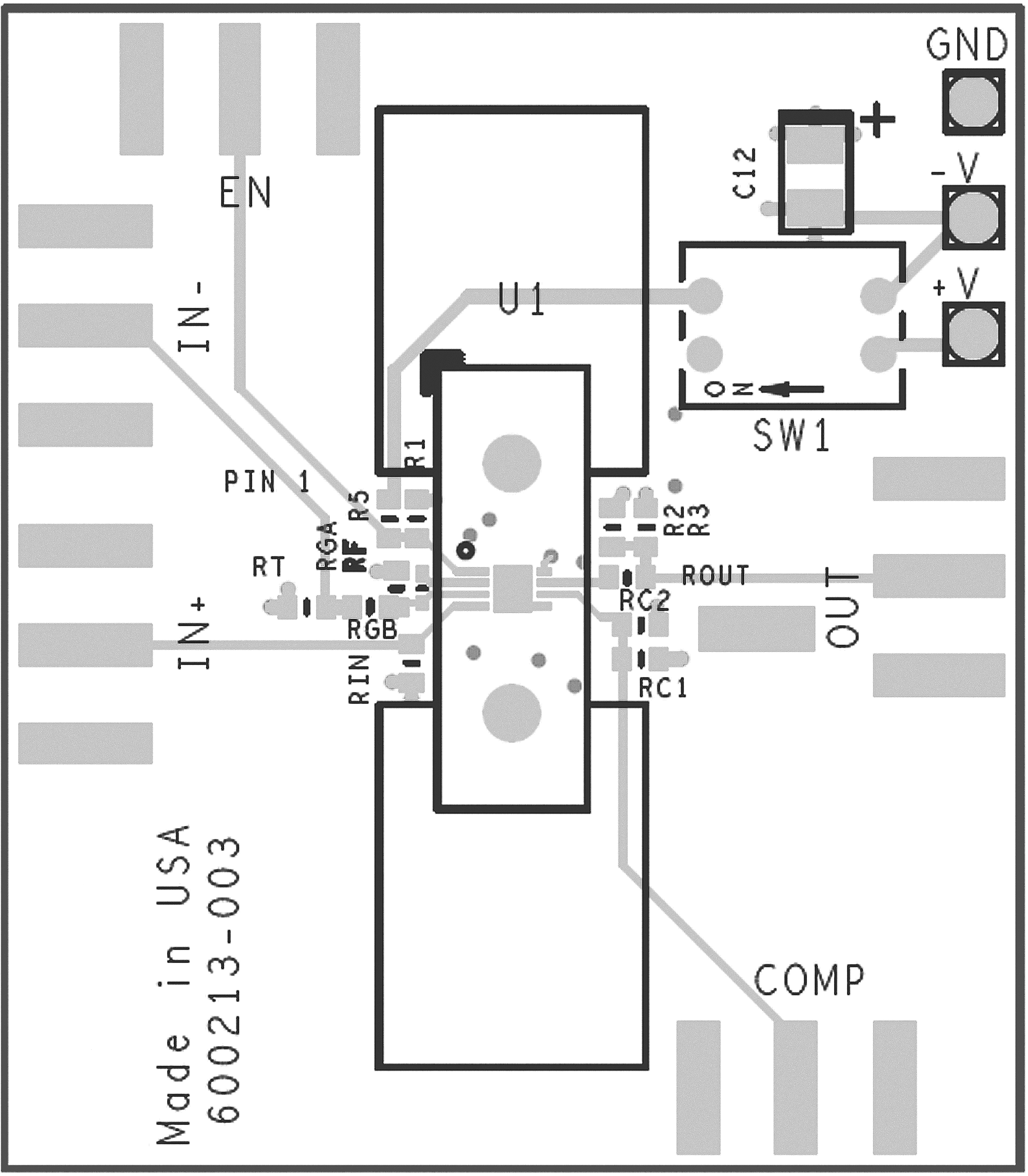 Figure 69. Evaluation Board Top Layer,
 WSON-8 Package
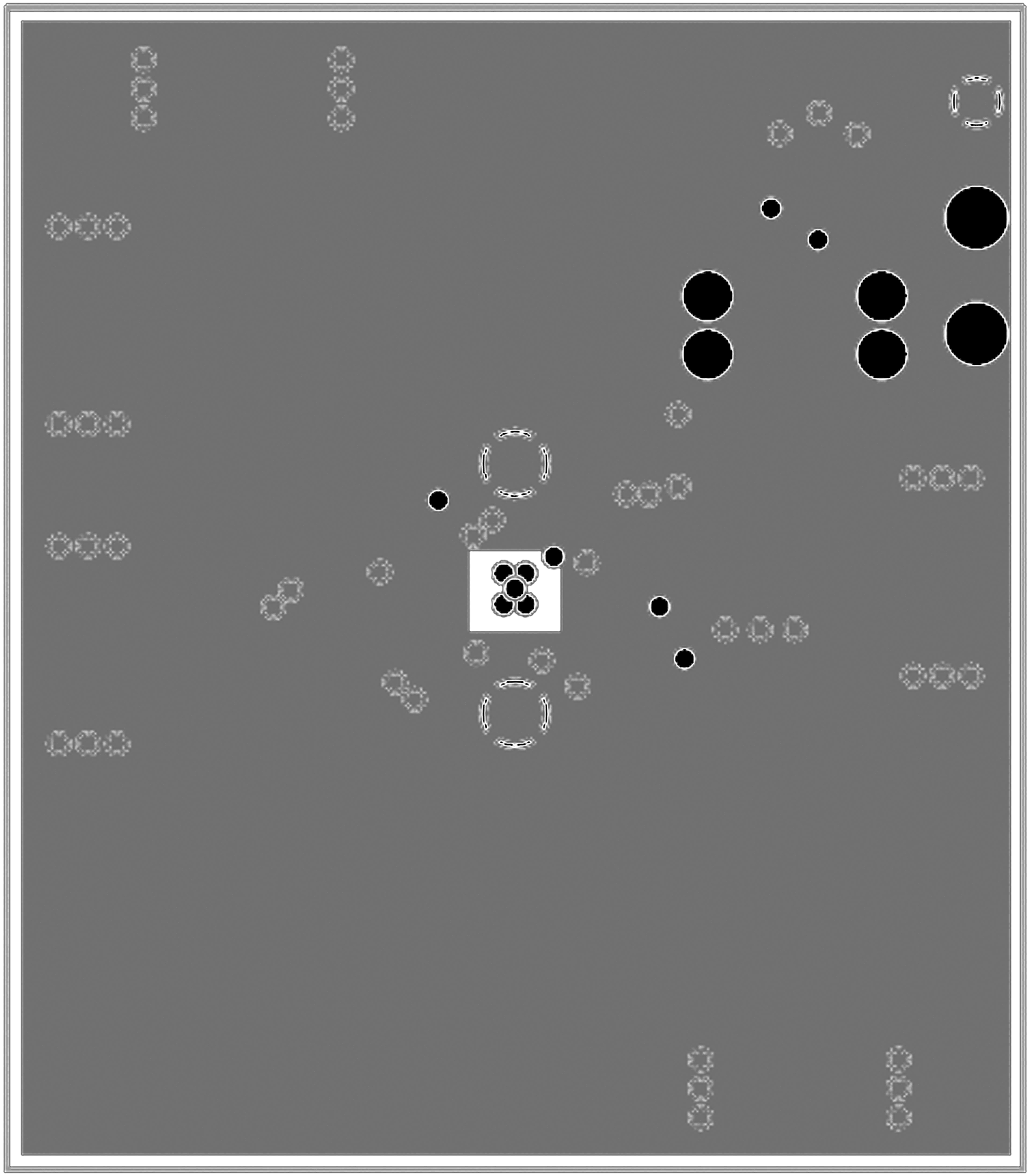 Figure 71. Evaluation Board Layer 2,
 WSON-8 Package
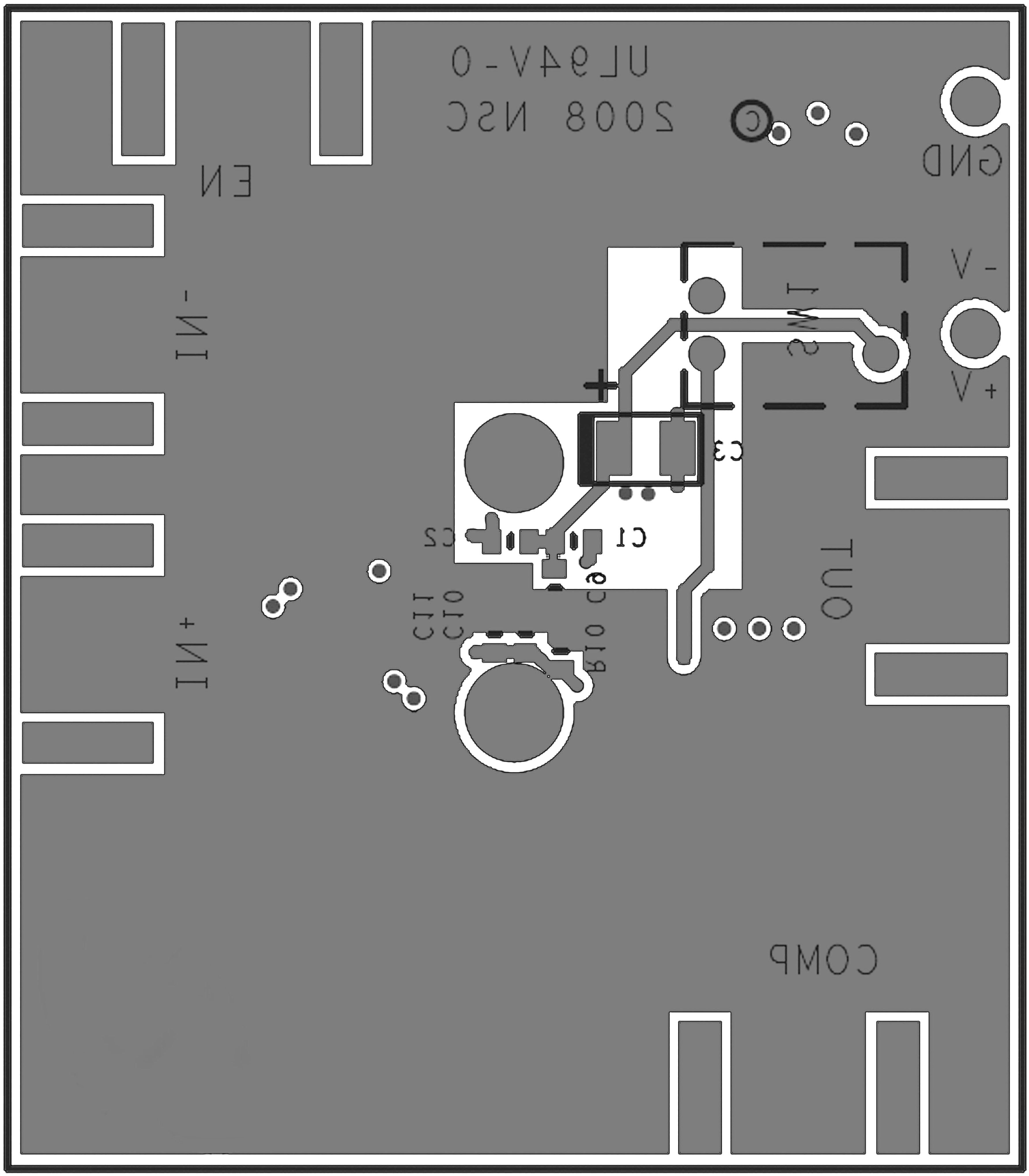 Figure 70. Evaluation Board Bottom Layer,
 WSON-8 Package
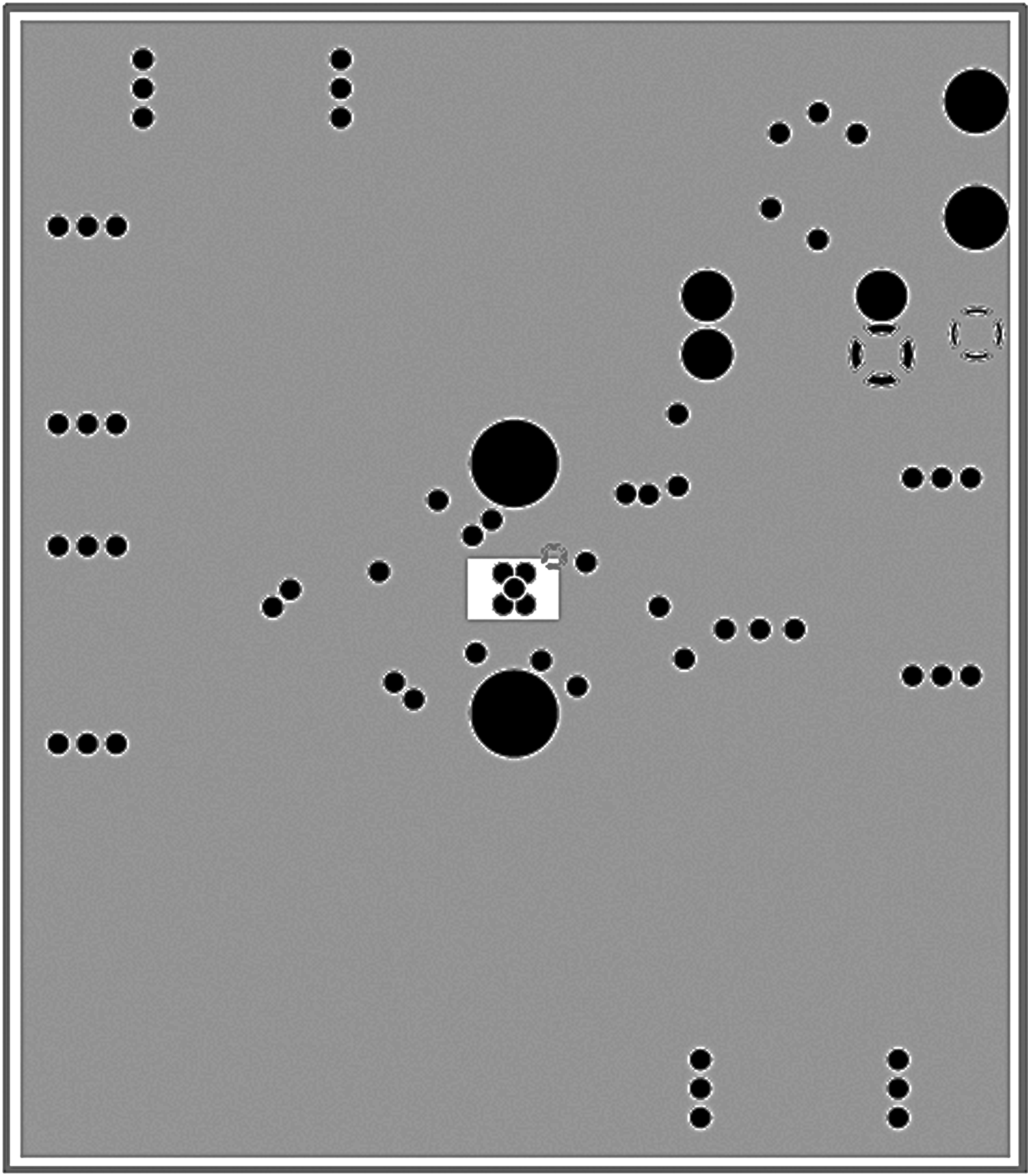 Figure 72. Evaluation Board Layer 3,
 WSON-8 Package