SNOSB18I April 2010 – December 2014 LMH6629
PRODUCTION DATA.
- 1 Features
- 2 Applications
- 3 Description
- 4 Revision History
- 5 Pin Configuration and Functions
- 6 Specifications
-
7 Detailed Description
- 7.1 Overview
- 7.2 Functional Block Diagram
- 7.3
Feature Description
- 7.3.1 WSON-8 Control Pins and SOT-23-5 Comparison
- 7.3.2 Compensation
- 7.3.3 Cancellation of Offset Errors Due to Input Bias Currents
- 7.3.4 Total Input Noise vs. Source Resistance
- 7.3.5 Noise Figure
- 7.3.6 Single-Supply Operation
- 7.3.7 Low-Noise Transimpedance Amplifier
- 7.3.8 Low-Noise Integrator
- 7.3.9 High-Gain Sallen-Key Active Filters
- 7.4 Device Functional Modes
- 8 Application and Implementation
- 9 Power Supply Recommendations
- 10Layout
- 11Device and Documentation Support
- 12Mechanical, Packaging, and Orderable Information
8 Application and Implementation
NOTE
Information in the following applications sections is not part of the TI component specification, and TI does not warrant its accuracy or completeness. TI’s customers are responsible for determining suitability of components for their purposes. Customers should validate and test their design implementation to confirm system functionality.
8.1 Application Information
The following discussion details some of the applications that can benefit from the LMH6629’s ultra-low noise, wide bandwidth, and single supply capability.
Note that It is essential to use a low-noise / low-distortion device to drive a high resolution ADC. This will minimize the impact on the quantization noise and to make sure that the driver’s distortion does not dominate the acquired data.
Equation 11 demonstrates the converter noise expression and Equation 12 shows the converter noise expression evaluated for the example depicted in Figure 66. Figure 67 shows a high-performance low-noise equalizer for such applications as magnetic tape channels using the LMH6629. Figure 68 shows the circuit’s simulated frequency response.
8.2 Typical Application
Many high-resolution data converters (ADC’s) require a differential input driver. In order to preserve the ADC’s dynamic range, the analog input driver must have a noise floor which is lower than the ADC’s noise floor. Figure 66 shows a ground referenced bipolar input (symmetrical swing around 0V) SE to differential converter used to drive a high resolution ADC. The combination of LMH6629’s low noise and the converter architecture reduces the impact on the ADC noise.
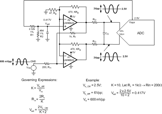 Figure 66. Low-Noise Single-Ended (SE) to Differential Converter
8.2.1 Design Requirements
For an ADC with N bits, the quantization Signal-to-noise ratio (SNR) is 6.02* N + 1.76 in dB. For example, a 12-bit ADC has a SNR of 74 dB (= 5000 V/V). Assuming a full-scale differential input of 2Vpp (0.707 V_RMS), the quantization oise referred to the ADC’s input is ~140 μV_RMS (= 0.707 V_RMS / 5000 V/V) over the bandwidth “visible” to the ADC. Assuming an ADC input bandwidth of 20 MHz, this translates to just 25 nV/RtHz (= 141 µV_RMS / SQRT(20 MHz * π/2)) noise density at the output of the driver. Using an amplifier to form the single-ended (SE) to Differential converter / driver for such an application is challenging, especially when there is some gain required. In addition, the input driver’s linearity (harmonic distortion) must also be high enough such that the spurs that get through to the ADC input are below the ADC’s LSB threshold or -73 dBc (= 20*log (1/ 212)) or lower in this case. Therefore, it is essential to use a low-noise / low-distortion device to drive a high resolution ADC in order to minimize the impact on the quantization noise and to make sure that the driver’s distortion does not dominate the acquired data.
8.2.2 Detailed Design Procedure
In the circuit depicted in Figure 66, the required gain dictates the resistor ratio “K”. With “K” and the driver output CM voltage (VO_CM) known, VSET can be established. Reasonable values for Rf and Rg can be set to complete the design.
In terms of output swing, with the LMH6629 output swing capability which requires ~0.85 V of headroom from either rail, the maximum total output swing into the ADC is limited to 6.6 VPP (=(5 – 2 x 0.85V) x 2); that is true with VO_CM set to mid-rail between V+ and V-. It should also be noted that the LMH6629’s input CMVR range includes the lower rail (V-) and that is the reason there is great flexibility in setting Vo_CM by controlling VSET. Another feature is that A1 and A2 inputs act like “virtual grounds” and thus do not see any signal swing. Note that due to the converter’s biasing, the source, VIN, needs to sink a current equal to VSET / RIN.
The converter example shown in Figure 66 operates with a noise gain of 6 (=1+ K / 2) and thus requires that the COMP pin to be tied low (WSON-8 package only). The 1st order approximated small signal bandwidth will be 280 MHz (=1.7 GHz / 6 V/V) which is computed using 1.7 GHz as the GBWP with COMP pin LO.
From a noise point of view, concentrating only on the dominant noise sources involved, here is the expression for the expected differential noise density at the input of the ADC.
Converter Noise Expression:

en is the LMH6629 input noise voltage and eRin_thermal is the thermal noise of RIN. The “23” and the “22” multipliers account for the different instances of each noise source (2 for en, and 1 for eRin_thermal).
Equation 11, evaluated for the circuit example of Figure 66, is shown in Equation 12:

Because of the LMH6629’s low input noise voltage (en), noise is dominated by the thermal noise of RIN. It is evident that the input resistor, RIN, can be reduced to lower the noise with lower input impedance as the trade-off.
8.2.2.1 Low-Noise Magnetic Media Equalizer
Figure 67 shows a high-performance low-noise equalizer for such applications as magnetic tape channels using the LMH6629. The circuit combines an integrator (used to limit noise) with a bandpass filter (used to boost the response centered at a frequency or over a band of interest) to produce the low-noise equalization. The circuit’s simulated frequency response is illustrated in Figure 68.
In this circuit, the bandpass filter center frequency is set by Equation 13:

For higher selectivity, use high C values; for wider bandwidth, use high L values, while keeping the product of L and C values the same to keep fc intact. The integrator’s -3dB roll-off is set by

If:

The integrator and the bandpass filter frequency interaction is minimized so that the operating frequencies of each can be set independently. Lowering the value of R2 increases the bandpass gain (boost) without affecting the integrator frequencies. With the LMH6629’s wide Gain Bandwidth (4 GHz), the center frequency could be adjusted higher without worries about loop gain limitation. This increases flexibility in tuning the circuit.
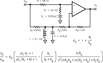 Figure 67. Low-Noise Magnetic Media Equalizer
8.2.3 Application Curves
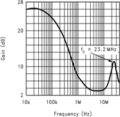 Figure 68. Equalizer Frequency Response