SNOSA42G November 2002 – December 2014 LMH6624 , LMH6626
PRODUCTION DATA.
- 1 Features
- 2 Applications
- 3 Description
- 4 Revision History
- 5 Pin Configuration and Functions
- 6 Specifications
- 7 Detailed Description
- 8 Application and Implementation
- 9 Power Supply Recommendations
- 10Layout
- 11Device and Documentation Support
- 12Mechanical, Packaging, and Orderable Information
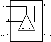
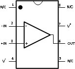
5 Pin Configuration and Functions
Package DBV
5-Pin SOT-23 (LMH6624)
Top View
Package D
8-Pin SOIC (LMH6624)
Top View
Package D or DGK
8-Pin SOIC Package D and VSSOP (LMH6626)
Top View
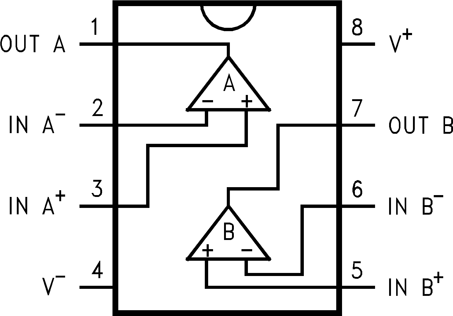
Pin Functions
| PIN | I/O | DESCRIPTION | |||
|---|---|---|---|---|---|
| NAME | NUMBER | ||||
| LMH6624 | LMH6626 | ||||
| DBV | D | DGK or D | |||
| -IN | 4 | 2 | – | I | Inverting Input |
| +IN | 3 | 3 | – | I | Non-inverting Input |
| IN A- | – | – | 2 | I | Inverting Input Channel A |
| IN B- | – | – | 6 | I | Inverting Input Channel B |
| IN A+ | – | – | 3 | I | Non-inverting Input Channel A |
| IN B+ | – | – | 5 | I | Non-inverting Input Channel B |
| N/C | – | 1, 5, 8 | – | –– | No Connection |
| OUT | 1 | 6 | – | O | Output |
| OUT A | – | – | 1 | O | Output Channel A |
| OUT B | – | – | 7 | O | Output Channel B |
| V- | 2 | 4 | 4 | I | Negative Supply |
| V+ | 5 | 7 | 8 | I | Positive Supply |