SNOSB30P October 2008 – January 2015 LMH6554
PRODUCTION DATA.
- 1 Features
- 2 Applications
- 3 Description
- 4 Typical Application Schematic
- 5 Revision History
- 6 Pin Configuration and Functions
- 7 Specifications
- 8 Detailed Description
- 9 Application and Implementation
- 10Power Supply Recommendations
- 11Layout
- 12Device and Documentation Support
- 13Mechanical, Packaging, and Orderable Information
10 Power Supply Recommendations
The LMH6554 can be used with any combination of positive and negative power supplies as long as the combined supply voltage is between 4.7 V and 5.25 V. The LMH6554 will provide best performance when the output voltage is set at the mid supply voltage, and when the total supply voltage is set to 5 V.
Power supply bypassing as shown in Power Supply Bypassing is important and power supply regulation should be within 5% or better.
10.1 Power Supply Bypassing
The LMH6554 requires supply bypassing capacitors as shown in Figure 36 and Figure 37. The 0.01-μF and 0.1-μF capacitors should be leadless SMT ceramic capacitors and should be no more than 3 mm from the supply pins. These capacitors should be star routed with a dedicated ground return plane or trace for best harmonic distortion performance. Thin traces or small vias will reduce the effectiveness of bypass capacitors. Also shown in both figures is a capacitor from the VCM and VEN pins to ground. These inputs are high impedance and can provide a coupling path into the amplifier for external noise sources, possibly resulting in loss of dynamic range, degraded CMRR, degraded balance and higher distortion.
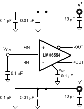 Figure 36. Split Supply Bypassing Capacitors
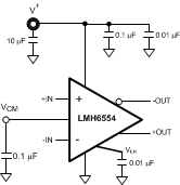 Figure 37. Single Supply Bypassing Capacitors