SNOSB30P October 2008 – January 2015 LMH6554
PRODUCTION DATA.
- 1 Features
- 2 Applications
- 3 Description
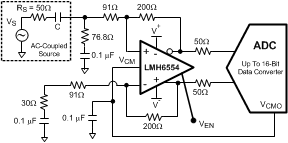
- 4 Typical Application Schematic
- 5 Revision History
- 6 Pin Configuration and Functions
- 7 Specifications
- 8 Detailed Description
- 9 Application and Implementation
- 10Power Supply Recommendations
- 11Layout
- 12Device and Documentation Support
- 13Mechanical, Packaging, and Orderable Information
1 Features
2 Applications
- Differential ADC Driver
- Single-Ended to Differential Converter
- High-Speed Differential Signaling
- IF/RF and Baseband Gain Blocks
- SAW Filter Buffer/Driver
- Oscilloscope Probes
- Automotive Safety Applications
- Video Over Twisted Pair
- Differential Line Driver
3 Description
The LMH6554 device is a high-performance fully differential amplifier designed to provide the exceptional signal fidelity and wide large-signal bandwidth necessary for driving 8- to 16-bit high-speed data acquisition systems. Using TI’s proprietary differential current mode input stage architecture, the LMH6554 has unity gain, small-signal bandwidth of 2.8 GHz and allows operation at gains greater than unity without sacrificing response flatness, bandwidth, harmonic distortion, or output noise performance.
The low-impedance differential output of the device is designed to drive ADC inputs and any intermediate filter stage. The LMH6554 delivers 16-bit linearity up to 75 MHz when driving 2-V peak-to-peak into loads as low as 200 Ω.
The LMH6554 is fabricated in TI's advanced complementary BiCMOS process and is available in a space-saving 14-lead UQFN package for higher performance.
Device Information(1)
| PART NUMBER | PACKAGE | BODY SIZE (NOM) |
|---|---|---|
| LMH6554 | UQFN (14) | 2.50 mm × 2.50 mm |
- For all available packages, see the orderable addendum at the end of the data sheet.
4 Typical Application Schematic