ZHCSH36 September 2017 LM73605 , LM73606
PRODUCTION DATA.
- 1 特性
- 2 应用
- 3 说明
- 4 修订历史记录
- 5 Pin Configuration and Functions
- 6 Specifications
-
7 Detailed Description
- 7.1 Overview
- 7.2 Functional Block Diagram
- 7.3
Feature Description
- 7.3.1 Synchronous Step-Down Regulator
- 7.3.2 Auto Mode and FPWM Mode
- 7.3.3 Fixed-Frequency Peak Current-Mode Control
- 7.3.4 Adjustable Output Voltage
- 7.3.5 Enable and UVLO
- 7.3.6 Internal LDO, VCC_UVLO, and BIAS Input
- 7.3.7 Soft Start and Voltage Tracking
- 7.3.8 Adjustable Switching Frequency
- 7.3.9 Frequency Synchronization and Mode Setting
- 7.3.10 Internal Compensation and CFF
- 7.3.11 Bootstrap Capacitor and VBOOT-UVLO
- 7.3.12 Power-Good and Overvoltage Protection
- 7.3.13 Overcurrent and Short-Circuit Protection
- 7.3.14 Thermal Shutdown
- 7.4 Device Functional Modes
-
8 Application and Implementation
- 8.1 Application Information
- 8.2
Typical Application
- 8.2.1 Design Requirements
- 8.2.2
Detailed Design Procedure
- 8.2.2.1 Custom Design With WEBENCH® Tools
- 8.2.2.2 Output Voltage Setpoint
- 8.2.2.3 Switching Frequency
- 8.2.2.4 Input Capacitors
- 8.2.2.5 Inductor Selection
- 8.2.2.6 Output Capacitor Selection
- 8.2.2.7 Feed-Forward Capacitor
- 8.2.2.8 Bootstrap Capacitors
- 8.2.2.9 VCC Capacitor
- 8.2.2.10 BIAS
- 8.2.2.11 Soft Start
- 8.2.2.12 Undervoltage Lockout Setpoint
- 8.2.2.13 PGOOD
- 8.2.3 Application Curves
- 9 Power Supply Recommendations
- 10Layout
- 11器件和文档支持
- 12机械、封装和可订购信息
8 Application and Implementation
NOTE
Information in the following applications sections is not part of the TI component specification, and TI does not warrant its accuracy or completeness. TI’s customers are responsible for determining suitability of components for their purposes. Customers should validate and test their design implementation to confirm system functionality.
8.1 Application Information
The LM73605/6 device is a step-down DC-DC voltage regulator. It is designed to operate with a wide supply voltage range (3.5 V to 36 V), wide switching frequency range (350 kHz to 2.2 MHz), and wide output voltage range: up to 95% VIN. is a synchronous converter with both HS and LS MOSFETs integrated, and it is capable of delivering a maximum output current of 5 A (LM73605) or 6 A (LM73606). The following design procedure can be used to select component values for the LM73605/6. Alternately, the WEBENCH® software may be used to generate a complete design. The WEBENCH® software uses an iterative design procedure and accesses a comprehensive database of components when generating a design (see Custom Design With WEBENCH® Tools). This section presents a simplified discussion of the design process.
8.2 Typical Application
The LM73605/6 only requires a few external components to perform high-efficiency power conversion, as shown in Simplified Schematic.
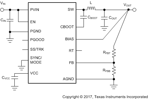 Figure 25. LM73605/6 Basic Schematic
The LM73605/6 also integrates many practical features to meet a wide range of system design requirements and optimization, such as UVLO, programmable soft-start time, start-up tracking, programmable switching frequency, clock synchronization and a power-good flag. Note that for ease of use, the feature pins do not require an additional component when not in use. They can be either left floating or shorted to ground. Please refer to Pin Configuration and Functions for details.
A comprehensive schematic with all features utilized is shown in Figure 26.
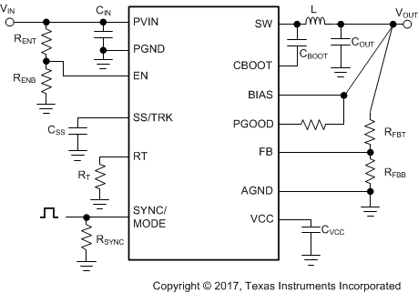 Figure 26. LM73605/6 Comprehensive Schematic with All Features Utilized
The external components must fulfill not only the needs of the power conversion, but also the stability criteria of the control loop. The LM73605/6 is optimized to work with a range of external components. For quick component selection, Table 3 can be used.
Table 3. Typical Component Selection
| fSW (kHz) | VOUT (V) | L (µH) | COUT (µF)(1) | RFBT (kΩ) | RFBB (kΩ) | RT (kΩ) |
| 350 | 1 | 2.2 | 500 | 100 | OPEN | 115 |
| 500 | 1 | 1.5 | 400 | 100 | OPEN | 78.7 or open |
| 1000 | 1 | 0.68 | 200 | 100 | OPEN | 39.2 |
| 2200 | 1 | 0.47 | 100 | 100 | OPEN | 17.4 |
| 350 | 3.3 | 4.7 | 200 | 100 | 43.5 | 115 |
| 500 | 3.3 | 3.3 | 150 | 100 | 43.5 | 78.7 or open |
| 1000 | 3.3 | 1.8 | 88 | 100 | 43.5 | 39.2 |
| 2200 | 3.3 | 1.2 | 44 | 100 | 43.5 | 17.4 |
| 350 | 5 | 6.8 | 120 | 100 | 25 | 115 |
| 500 | 5 | 4.7 | 88 | 100 | 25 | 78.7 or open |
| 1000 | 5 | 3.3 | 66 | 100 | 25 | 39.2 |
| 2200 | 5 | 2.2 | 44 | 100 | 25 | 17.4 |
| 350 | 12 | 15 | 66 | 100 | 9.1 | 115 |
| 500 | 12 | 10 | 44 | 100 | 9.1 | 78.7 or open |
| 1000 | 12 | 6.8 | 22 | 100 | 9.1 | 39.2 |
| 350 | 24 | 22 | 40 | 100 | 4.3 | 115 |
| 500 | 24 | 15 | 30 | 100 | 4.3 | 78.7 or open |
8.2.1 Design Requirements
Detailed design procedure is described based on a design example. For this design example, use the parameters listed in Table 4.
Table 4. Design Example Parameters
| DESIGN PARAMETER | VALUE |
| Typical input voltage | 12 V |
| Output voltage | 5 V |
| Output current | 5 A |
| Operating frequency | 500 kHz |
| Soft-start time | 11 ms |
8.2.2 Detailed Design Procedure
8.2.2.1 Custom Design With WEBENCH® Tools
To create a custom design with the WEBENCH® Power Designer, click the LM73605 or LM73606 device.
- Start by entering the input voltage (VIN), output voltage (VOUT), and output current (IOUT) requirements.
- Optimize the design for key parameters such as efficiency, footprint, and cost using the optimizer dial.
- Compare the generated design with other possible solutions from Texas Instruments.
The WEBENCH Power Designer provides a customized schematic along with a list of materials with real-time pricing and component availability.
In most cases, these actions are available:
- Run electrical simulations to see important waveforms and circuit performance
- Run thermal simulations to understand board thermal performance
- Export customized schematic and layout into popular CAD formats
- Print PDF reports for the design, and share the design with colleagues
Get more information about WEBENCH tools at www.ti.com/WEBENCH.
8.2.2.2 Output Voltage Setpoint
The output voltage of the LM73605/6 device is externally adjustable using a resistor divider network. The divider network is comprised of top feedback resistor RFBT and bottom feedback resistor RFBB. Use Equation 24 to determine the output voltage of the converter.

Typically, RFBT = 10 kΩ to 100 kΩ is recommended. Larger RFBT and RFBB values reduce the quiescent current going through the divider, which help maintain high efficiency at very light loads. But larger divider values also make the feedback path more susceptible to noise. If efficiency at very light loads is critical in a certain application, RFBT up to 1 MΩ can be used.

RFBT = 100 kΩ is selected here. RFBB = 24.99 kΩ can be calculated to get 5-V output voltage.
8.2.2.3 Switching Frequency
The default switching frequency of the LM73605/6 device is set at 500 kHz. For this design, the RT pin can be floating, and the LM73605/6 switches at 500 kHz in CCM mode. An RT resistor of 78.7 kΩ, calculated using Equation 13, Figure 21, or Table 1, can be connected from RT pin to ground to obtain 500-kHz operation frequency as well.
The LM73605/6 switching action can synchronize to an external clock from 350 kHz to 2.2 MHz. TI recommends connecting an external clock to the SYNC/MODE pin with a 50-Ω to 100-Ω termination resistor. The SYNC/MODE pin must be grounded if not used.
RT pin is floating and SYNC/MODE pin is tied to ground in this design.
8.2.2.4 Input Capacitors
The LM73605/6 device requires high-frequency ceramic input decoupling capacitors. Depending on the application, a bulk input capacitor can also be added. The typical recommended ceramic decoupling capacitors include one small, 0.1 µF to 1 µF, and one large, 10 µF to 22 µF, capacitors. TI recommends high-quality ceramic type X5R or X7R capacitors. The voltage rating must be greater than the maximum input voltage. As a general rule, to compensate the derating TI recommends a voltage rating of twice the maximum input voltage.
It is very important in buck regulator to place the small decoupling capacitor right next to the PVIN and PGND pins. This capacitor is used to bypass the high frequency switching noise by providing a return path of the noise. It prevents the noise from spreading to wider area of the board. The large bypass ceramic capacitor must also be as close as possible to the PVIN and PGND pins.
Additionally, some bulk capacitance may be required, especially if the LM73605/6 circuit is not located within approximately 2 inches from the input voltage source. This capacitor is used to provide damping to the voltage spike due to the lead inductance of the cable. The optimum value for this capacitor is four times the ceramic input capacitance with ESR close to the characteristic impedance of the LC filter formed by your input inductance and your ceramic input capacitors. It is not critical that the electrolytic filter be at the optimum value for damping, but it must be rated to handle the maximum input voltage including ripple voltage.
For this design, two 10-µF, X7R dielectric capacitors rated for 50 V are used for the input decoupling capacitance, and a capacitor with a value of 0.47 µF for high-frequency filtering.
NOTE
DC bias effect: High capacitance ceramic capacitors have a DC bias derating effect, which will have a strong influence on the final effective capacitance. Therefore, the right capacitor value has to be chosen carefully. Package size and voltage rating in combination with dielectric material are responsible for differences between the rated capacitor value and the effective capacitance.
8.2.2.5 Inductor Selection
The first criterion for selecting an output inductor is the inductance. In most buck converters, this value is based on the desired peak-to-peak ripple current in the inductor, ILripple. An inductance that gives a ripple current of 10% to 30% of the maximum output current (5 A or 6 A) is a good starting point. The inductance can be calculated from Equation 26:

where
- ILripple = (0.1 to 0.3) × IL_MAX
- IL_MAX = 5 A for LM73605 and 6 A for LM73606
- D = VOUT / VIN
Selected ILripple is between 10% to 30% of the rated current of the device.
As with switching frequency, the selection of the inductor is a tradeoff between size, cost, and performance. Higher inductance gives lower ripple current and hence lower output voltage ripple. With peak current mode control, the current ripple is the input signal to the control loop. A certain amount of ripple current is needed to maintain the signal-to-noise ratio of the control loop. Within the same series (same size/height), a larger inductance will have a higher series resistance (ESR). With similar ESR, size and/or height will be greater. Larger inductance also has slower current slew rate during large load transients.
Lower inductance usually results in a smaller, less expensive component; however, the current ripple will be higher, thus more output capacitor is needed to maintain the same amount of output voltage ripple. The RMS current is higher with the same load current due to larger ripple. The switching loss is higher because the switch current, which is the peak current, is higher when the HS switch turns off and LS switch turns on. Core loss of the inductor is also larger with higher ripple. Core loss needs to be considered, especially with higher switching frequencies. Check the ripple current over VIN_MIN to VIN_MAX range to make sure current ripple is reasonable over entire supply voltage range.
For applications with large VOUT and typical VOUT / VIN > 50%, sub-harmonic oscillation can be a concern in peak current-mode-controlled buck converters. Select inductance so that
where
- N = 3 with LM73605
- N = 3.6 with LM73606
The second criterion is inductor saturation current rating. Because the maximum inductor current is limited by the high-side switch current limit, it is advised to select an inductor with a saturation current higher than the ILIMIT-HS. TI recommends selection of soft saturation inductors. A power inductor could be the major source of radiated noise. When EMI is a concern in the application, select a shielded inductor, if possible.
For this design, 20% ripple of 5 A yields 5.8-µH inductance. A 4.7-µH inductor is selected, which gives 25% ripple current.
8.2.2.6 Output Capacitor Selection
The output capacitor is responsible for filtering the inductor current, and supplying load current during transients. Capacitor selection depends on application conditions as well as ripple and transient requirements. Best performance is achieved by using ceramic capacitors or combinations of ceramic and other types of capacitors. For high output voltage conditions, such as 12 V and above, finding ceramic capacitors that are rated for an appropriate voltage becomes challenging. In such cases choose a low-ESR SP-CAP™ or POSCAP™-type capacitor. It is a good idea to use a low-value ceramic capacitor in parallel with other capacitors, to bypass high frequency noise between ground and VOUT.
For a given input and output requirement, Equation 28 gives an approximation for a minimum output capacitor required.

where
- r = Ripple ratio of the inductor ripple current (ILripple / 5 A or 6 A)
- ΔVOUT = Target output voltage undershoot, for example, 5% to 10% of VOUT
- D’ = 1 – duty cycle
- fSW = switching frequency
- IOUT = load current
Along with Equation 28, for the same requirement calculate the maximum ESR with Equation 29.

The output capacitor is also the dominating factor in the loop response of a peak-current mode controlled buck converter. A simplified estimation of the control loop crossover frequency can be found by Equation 18.
Select COUT so that the fX is no higher than 1/6 of the switching frequency. Typically, fX / fSW = 1/10 to 1/8 provides a good combination of stability and performance.
For this design, one 0.47-µF, 50-V X7R and four 22-µF, 16-V, X7R ceramic capacitors are used in parallel.
8.2.2.7 Feed-Forward Capacitor
The LM73605/6 is internally compensated. Typically, select RFBT ≤ 100 kΩ, then CFF is not needed. When very low quiescent current is needed, RFBT = 1 MΩ may be used. If COUT is mainly ceramic type low ESR capacitors, an external feed-forward capacitor CFF may be needed to improve the phase margin. Add CFF in parallel with RFBT. CFF is chosen such that the phase boost is maximized at the estimated crossover frequency fX. Equation 21 was tested.
With this design, because RFBT = 100 kΩ is selected, no CFF is needed.
8.2.2.8 Bootstrap Capacitors
Every LM73605/6 design requires a bootstrap capacitor, CBOOT. The recommended bootstrap capacitor is 0.47 µF and rated at 6.3 V or greater. The bootstrap capacitor is located between the SW pin and the CBOOT pin. The bootstrap capacitor must be a high-quality ceramic type with X7R or X5R grade dielectric for temperature stability.
8.2.2.9 VCC Capacitor
The VCC pin is the output of an internal LDO for LM73605/6. The input for this LDO comes from either VIN or BIAS pin voltage. The recommended CVCC capacitor is 2.2 µF and rated at 6.3 V or greater. It must be a high-quality ceramic type with X7R or X5R grade to insure stability. Never short VCC pin to ground during operation.
8.2.2.10 BIAS
Because VOUT = 5 V in this design, the BIAS pin is tied to VOUT to reduce LDO power loss. The output voltage is supplying the LDO current instead of the input voltage. The power saving is ILDO × (VIN – VOUT). The power saving is more significant when VIN >> VOUT and with higher frequency operation. To prevent VOUT noise and transients from coupling to BIAS, a series resistor, 1 Ω to 10 Ω, may be added between VOUT and BIAS. A bypass capacitor with a value of 1 μF or higher can be added close to the BIAS pin to filter noise.
8.2.2.11 Soft Start
The SS/TRK pin can be floating to start up following the internal soft-start ramp. In order to extend the soft-start time, an external soft-start capacitor can be used. Use Equation 12 in order to calculate the soft-start capacitor value.
With a desired soft-start time tSS = 11 ms, a soft-start charging current of ISSC = 2 µA (typical), and VFB = 1.006 V (typical), Equation 12 yields a soft-start capacitor value of 22 nF.
8.2.2.12 Undervoltage Lockout Setpoint
The system undervoltage lockout (UVLO) is adjusted using the external voltage divider network of RENT and RENB. With one selected RENT value, RENB can be found by Equation 10.
Note that the divider adds to supply quiescent current by VIN / (RENT + RENB). Small RENT and RENB values add more quiescent current loss. However, large divider values make the node more sensitive to noise.
In this design, EN pin is tied to PVIN pin with a 100-kΩ resistor.
8.2.2.13 PGOOD
For this design, a 100-kΩ resistor is used to pull up PGOOD to VOUT.
8.2.3 Application Curves

| VOUT = 3.3 V | fSW = 500 kHz | Auto Mode |
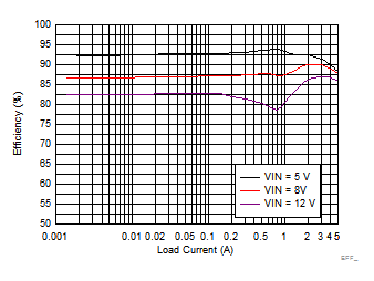
| VOUT = 3.3 V | fSW = 2200 kHz | Auto Mode |
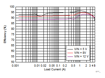
| VOUT = 3.3 V | fSW = 350 kHz | Auto Mode |
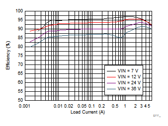
| VOUT = 5 V | fSW = 500 kHz | Auto Mode |
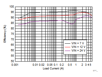
| VOUT = 5 V | fSW = 1000 kHz | Auto Mode |
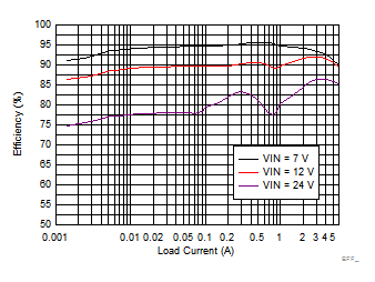
| VOUT = 5 V | fSW = 2200 kHz | Auto Mode |
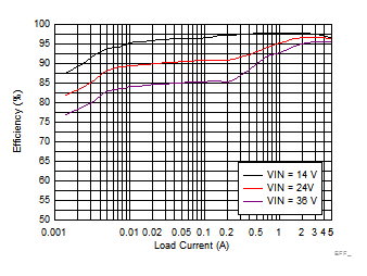
| VOUT = 12 V | fSW = 500 kHz | Auto Mode |
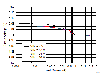
| VOUT = 5 V | fSW = 500 kHz | Auto Mode |
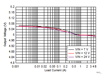
| VOUT = 5 V | fSW = 2200 kHz | Auto Mode |
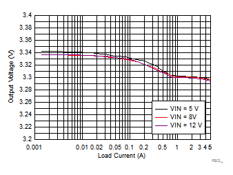
| VOUT = 3.3 V | fSW = 2200 kHz | Auto Mode |
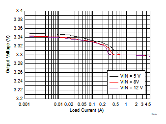
| VOUT = 3.3 V | fSW = 500 kHz | Auto Mode |
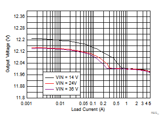
| VOUT = 12 V | fSW = 500 kHz | Auto Mode |
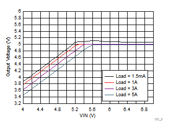
| VOUT = 5 V | fSW = 2200 kHz | Auto Mode |
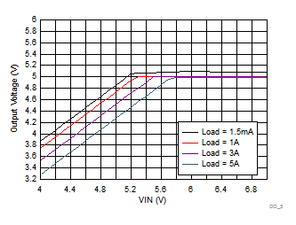
| VOUT = 5 V | fSW = 500 kHz | Auto Mode |
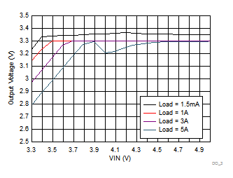
| VOUT = 3.3 V | fSW = 500 kHz | Auto Mode |
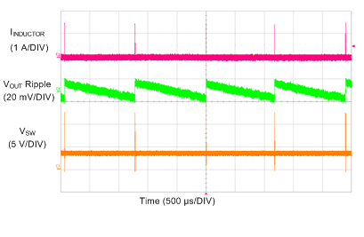
| VIN = 12 V | VOUT = 3.3 V | fSW = 500 kHz |
| IOUT = 1 mA | Auto Mode |
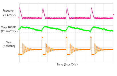
| VIN = 12 V | VOUT = 3.3 V | fSW = 500 kHz |
| IOUT = 100 mA | Auto Mode |
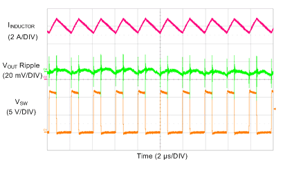
| VIN = 12 V | VOUT = 3.3 V | fSW = 500 kHz |
| IOUT = 6 A | Auto Mode |
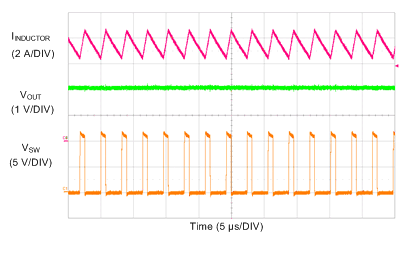
| VIN = 12 V | VOUT set at 3.3 V | fSW set at 500 kHz |
| IOUT = 7.5 A | VOUT droops to 2 V |
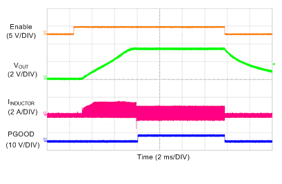
| VIN = 12 V | VOUT = 3.3 V | fSW = 500 kHz |
| IOUT= 200 mA | FPWM Mode |
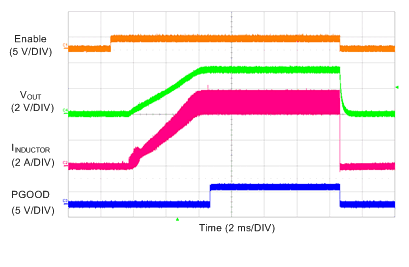
| VIN = 12 V | VOUT = 3.3 V | fSW = 500 kHz |
| IOUT = 5 A | Auto Mode |
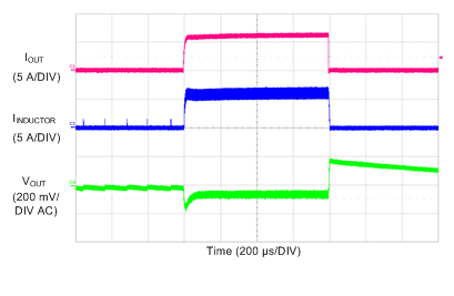
| VIN = 12 V | VOUT = 3.3 V | fSW = 500 kHz |
| IOUT = 10 mA to 6 A to 10 mA | Auto Mode | |
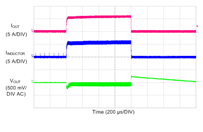
| VIN = 12 V | VOUT = 5 V | fSW = 2200 kHz |
| IOUT = 10 mA to 5 A to 10 mA | Auto Mode | |
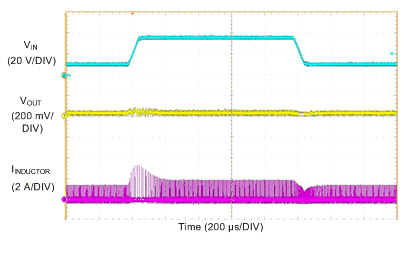
| IOUT = 100 mA | VOUT = 3.3 V | fSW = 500 kHz |
| VIN = 10 V to 35 V to 10 V | Auto Mode | |
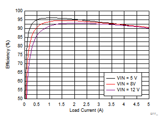
| VOUT = 3.3 V | fSW = 500 kHz | FPWM Mode |
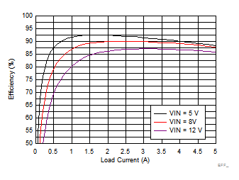
| VOUT = 3.3 V | fSW = 2200 kHz | FPWM Mode |
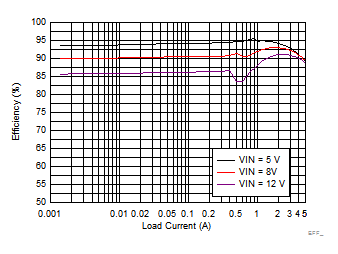
| VOUT = 3.3 V | fSW = 1000 kHz | Auto Mode |
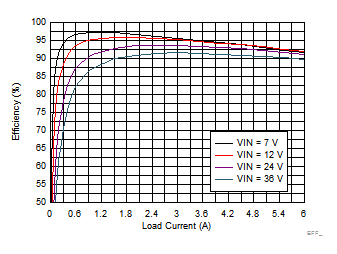
| VOUT = 5 V | fSW = 500 kHz | FPWM Mode |
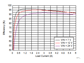
| VOUT = 5 V | fSW = 1000 kHz | FPWM Mode |
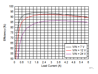
| VOUT = 5 V | fSW = 2200 kHz | FPWM Mode |
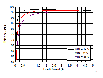
| VOUT = 12 V | fSW = 500 kHz | FPWM Mode |
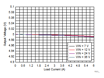
| VOUT = 5 V | fSW = 500 kHz | FPWM Mode |
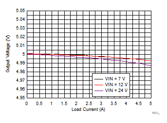
| VOUT = 5 V | fSW = 2200 kHz | FPWM Mode |
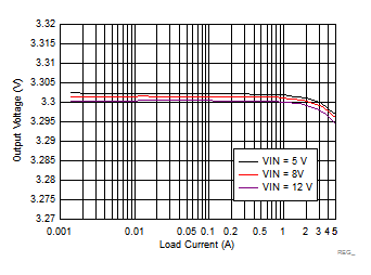
| VOUT = 3.3 V | fSW = 2200 kHz | FPWM Mode |
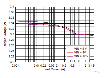
| VOUT = 3.3 V | fSW = 1000 kHz | Auto Mode |
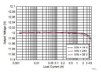
| VOUT = 12 V | fSW = 500 kHz | FPWM Mode |
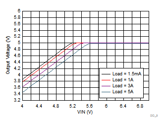
| VOUT = 5 V | fSW = 2200 kHz | FPWM Mode |

| VOUT = 5 V | fSW = 1000 kHz | Auto Mode |
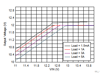
| VOUT = 12 V | fSW = 500 kHz | Auto Mode |
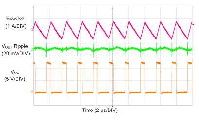
| VIN = 12 V | VOUT = 3.3 V | fSW = 500 kHz |
| IOUT = 1 mA | FPWM Mode |
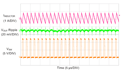
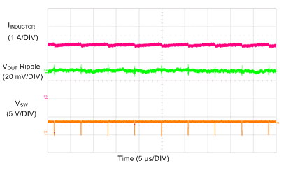
| VIN = 12 V | VOUT = 3.3 V | fSW = 500 kHz |
| IOUT = 100 mA | FPWM Mode |
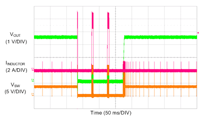
| VIN = 3.66 V | VOUT = 3.3 V | fSW set at 500 kHz |
| IOUT = 3 A | Auto Mode |
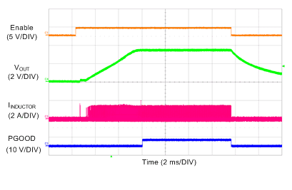
| VIN = 12 V | VOUT = 3.3 V | fSW = 500 kHz |
| VIN = 12 V | VOUT = 3.3 V | fSW = 500 kHz |
| IOUT= 200 mA | Auto Mode |
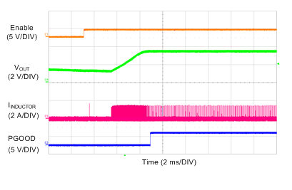
| VIN = 12 V | VOUT = 3.3 V | fSW = 500 kHz |
| VPRE-BIAS= 1.5 V | Auto Mode |
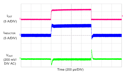
| VIN = 12 V | VOUT = 3.3 V | fSW = 500 kHz |
| IOUT = 10 mA to 6 A to 10 mA | FPWM Mode | |
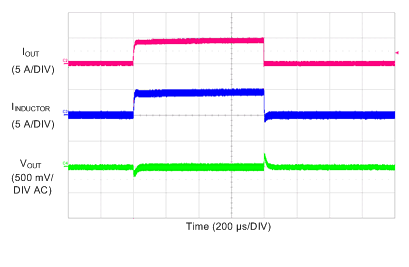
| VIN = 12 V | VOUT = 5 V | fSW = 2200 kHz |
| IOUT = 10 mA to 5 A to 10 mA | FPWM Mode | |
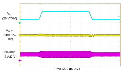
| IOUT = 2 A | VOUT = 3.3 V | fSW = 500 kHz |
| VIN = 10 V to 35 V to 10 V | Auto Mode | |