ZHCSH36 September 2017 LM73605 , LM73606
PRODUCTION DATA.
- 1 特性
- 2 应用
- 3 说明
- 4 修订历史记录
- 5 Pin Configuration and Functions
- 6 Specifications
-
7 Detailed Description
- 7.1 Overview
- 7.2 Functional Block Diagram
- 7.3
Feature Description
- 7.3.1 Synchronous Step-Down Regulator
- 7.3.2 Auto Mode and FPWM Mode
- 7.3.3 Fixed-Frequency Peak Current-Mode Control
- 7.3.4 Adjustable Output Voltage
- 7.3.5 Enable and UVLO
- 7.3.6 Internal LDO, VCC_UVLO, and BIAS Input
- 7.3.7 Soft Start and Voltage Tracking
- 7.3.8 Adjustable Switching Frequency
- 7.3.9 Frequency Synchronization and Mode Setting
- 7.3.10 Internal Compensation and CFF
- 7.3.11 Bootstrap Capacitor and VBOOT-UVLO
- 7.3.12 Power-Good and Overvoltage Protection
- 7.3.13 Overcurrent and Short-Circuit Protection
- 7.3.14 Thermal Shutdown
- 7.4 Device Functional Modes
-
8 Application and Implementation
- 8.1 Application Information
- 8.2
Typical Application
- 8.2.1 Design Requirements
- 8.2.2
Detailed Design Procedure
- 8.2.2.1 Custom Design With WEBENCH® Tools
- 8.2.2.2 Output Voltage Setpoint
- 8.2.2.3 Switching Frequency
- 8.2.2.4 Input Capacitors
- 8.2.2.5 Inductor Selection
- 8.2.2.6 Output Capacitor Selection
- 8.2.2.7 Feed-Forward Capacitor
- 8.2.2.8 Bootstrap Capacitors
- 8.2.2.9 VCC Capacitor
- 8.2.2.10 BIAS
- 8.2.2.11 Soft Start
- 8.2.2.12 Undervoltage Lockout Setpoint
- 8.2.2.13 PGOOD
- 8.2.3 Application Curves
- 9 Power Supply Recommendations
- 10Layout
- 11器件和文档支持
- 12机械、封装和可订购信息
7 Detailed Description
7.1 Overview
The LM73605/6 is an easy-to-use synchronous step-down DC-DC converter that operates from a 3.5-V to 36-V supply voltage. It is capable of delivering up to 5-A (LM73605) or 6-A (LM73606) DC load current with exceptional efficiency and thermal performance in a very small solution size.
The LM73605/6 employs fixed-frequency peak current-mode control with configurable auto or FPWM operation mode. Auto mode provides very high efficiency at light loads, and FPWM mode maintains constant switching frequency over entire load range.
The device is internally compensated, which reduces design time and the number of external components. The switching frequency is programmable from 350 kHz to 2.2 MHz by an external resistor. The LM73605/6 can also synchronize to an external clock within the same frequency range. The wide switching frequency range allows the device to be optimized for a wide range of system requirements. It can be optimized for small solution size with higher frequency; or for high efficiency with lower switching frequency. The LM73605/6 has very low quiescent current, which is critical for battery operated systems. It allows for a wide range of voltage conversion ratios due to very small minimum ON-time (tON-MIN) and minimum OFF-time (tOFF-MIN). Automated frequency foldback is employed at very high or low duty cycles to further extend the operating range.
The LM73605/6 also features a power-good (PGOOD) flag, precision enable, internal or adjustable soft start, pre-biased start-up, and output voltage tracking. Protection features include thermal shutdown, undervoltage lockout (UVLO), cycle-by-cycle current limiting, and short-circuit hiccup protection. It provides flexible and easy-to-use solutions for a wide range of applications.
The family requires very few external components and has a pin out designed for simple, optimum PCB layout for enhanced EMI and thermal performance. The LM73605/6 device is available in a 30-pin WQFN leadless package.
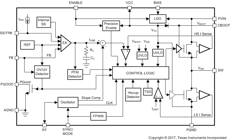
7.2 Functional Block Diagram
7.3 Feature Description
7.3.1 Synchronous Step-Down Regulator
The LM73605/6 is a synchronous buck converter with both power MOSFETs integrated in the device. Figure 10 shows a simplified schematic for synchronous and non-synchronous buck converters. The synchronous buck integrates both high-side (HS) and low-side (LS) power MOSFETs. The non-synchronous buck integrates HS MOSFET and works with a discrete power diode as LS rectifier.
 Figure 10. Simplified Synchronous vs Non-synchronous Buck Converters
A synchronous converter with integrated HS and LS MOSFETs offers benefits such as less design effort, lower external components count, reduced total solution size, higher efficiency at heavier load, easier PCB design, and more control flexibility.
The main advantage of a synchronous converter is that the voltage drop across the LS MOSFET is lower than the voltage drop across the power diode of a non-synchronous converter. Lower voltage drop translates into less power dissipation and higher efficiency. The LM73605/6 integrates HS and LS MOSFETs with very low on-time resistance to improve efficiency. It is especially beneficial when the output voltage is low. Because the LS MOSFET is integrated into the device, at light loads a synchronous converter has the flexibility to operate in either discontinuous or continuous conduction mode.
An integrated LS MOSFET also allows the controller to obtain inductor current information when the LS switch is on. It allows the control loop to make more complex decisions based on HS and LS currents. It allows the LM73605/6 to have peak and valley cycle-by-cycle current limiting for more robust protection.
7.3.2 Auto Mode and FPWM Mode
The LM73605/6 has configurable auto mode or FPWM options.
In auto mode, the device operates in diode emulation mode (DEM) at light loads. In DEM, inductor current stops flowing when it reaches 0 A. This is also referred to as discontinuous conduction mode (DCM). This is the same behavior as the non-synchronous regulator, with higher efficiency. At heavier load, when the inductor current valley is above 0 A, the device operates in continuous conduction mode (CCM), where the switching frequency is fixed and set by RT pin.
In auto mode, the peak inductor current has a minimum limit, IPEAK_MIN, in the LM73605/6. When peak current reaches IPEAK_MIN, the switching frequency reduces to regulate the required load current. Switching frequency lowers when load reduces. This is when the device operates in pulse frequency modulation (PFM). PFM further improves efficiency by reducing switching losses. Light load efficiency is especially important for battery operated systems.
In forced PWM (FPWM) mode, the device operates in CCM regardless of load with the frequency set by RT pin or synchronization input. Inductor current can go negative at light loads. At light loads, the efficiency is lower than auto mode, due to higher conduction losses and switching losses. In FPWM, the device has fixed switching frequency over the entire load range, which is beneficial to noise sensitive applications.
Figure 11 shows the inductor current waveforms in each mode with heavy load, light load, and very light load. The difference between the two modes is at lighter loads where inductor current valley reaches zero.
 Figure 11. Inductor Current Waveforms at Auto Mode and FPWM Mode with Different Loads
In CCM, the inductor current peak-to-peak ripple can be estimated by Equation 1:

The average or DC value of the inductor current equals the load current, or output current IOUT, in steady state. Peak inductor current can be calculated by Equation 2
Valley inductor current can be calculated by Equation 3
In auto mode, the CCM to DCM boundary condition is when IVALLEY = 0 A. When ILripple ≥ IPEAK_MIN, the load current at the DCM boundary condition can be found by Equation 4. When the peak-to-peak ripple current is smaller than ILripple ≥ IPEAK-MIN, the PFM boundary will be reached first.
where
- ILripple ≥ IPEAK_MIN
In auto mode, the PFM operation boundary condition is when IPEAK = IPEAK_MIN. Frequency foldback occurs when peak current drops to IPEAK_MIN, no matter whether in CCM or DCM operation. When current ripple is small, ILripple < IPEAK_MIN, the peak current reaches IPEAK_MIN when still in CCM. The output current at CCM PFM boundary can be found by Equation 5
where
- ILripple < IPEAK-MIN
The current ripple increases with reduced frequency if load reduces. When valley current reaches zero, the frequency continues to fold back with constant peak current and discontinuous current.
In FPWM mode, there is no IPEAK-MIN limit. The peak current is defined by Equation 2 at light loads and heavy loads.
See Frequency Synchronization and Mode Setting for mode setting options in LM73605/6. Mode setting only affects operation at light loads. There is no difference if load current is above the DCM and PFM boundary conditions discussed above.
7.3.3 Fixed-Frequency Peak Current-Mode Control
The LM73605/6 synchronous switched mode voltage regulator employs fixed frequency peak current mode control with advanced features. The fixed switching frequency is controlled by an internal clock. To get accurate DC load regulation, a voltage feedback loop is implemented to generate peak current command. The HS switch is turned on at the rising edge of the clock. As shown in Figure 12, during the HS switch on-time tON, the SW pin voltage VSW swings up to approximately VIN, and the inductor current IL increases with a linear slope. The HS switch is turned off when the inductor current reaches the peak current command. During the HS switch off-time tOFF, the LS switch is turned on. Inductor current discharges through the LS switch, which forces the VSW to swing below ground by the voltage drop across the LS switch. The LS switch is turned off at the next clock cycle, before the HS switch is turned on. The regulation loop adjusts the peak current command to maintain a constant output voltage.
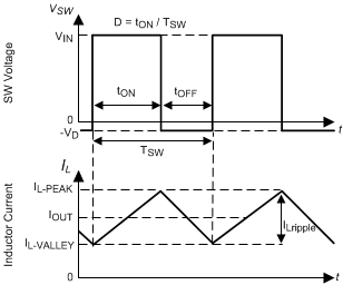 Figure 12. SW Voltage and Inductor Current Waveforms in CCM
Duty cycle D is defined by the on-time of the HS switch over the switching period:
where
- TSW = 1 / fSW is the switching period
In an ideal buck converter, where losses are ignored, D is proportional to the output voltage and inverse proportional to the input voltage: D = VOUT ⁄ VIN.
When the LM73605/6 is set to operate in auto mode, the LS switch is turned off when its current reaches zero ampere before the next clock cycle comes. Both HS switch and LS switch are off before the HS switch is turned on at the next clock cycle.
7.3.4 Adjustable Output Voltage
The voltage regulation loop in the LM73605/6 regulates the FB pin voltage to be the same as the internal reference voltage. The output voltage of the LM73605/6 is set by a resistor divider to program the ratio from VOUT to VFB. The resistor divider is connected from the output to ground with the mid-point connecting to the FB pin.
 Figure 13. Output Voltage Setting by Resistor Divider
The internal voltage reference and feedback loop produce precise voltage regulation over temperature. TI recommends using divider resistors with 1% tolerance or better, and with temperature coefficient of 100 ppm or lower. Typically, RFBT = 10 kΩ to 100 kΩ is recommended. Larger RFBT and RFBB values reduce the quiescent current going through the divider, which help maintain high efficiency at very light load. But larger divider values also make the feedback path more susceptible to noise. If efficiency at very light load is critical in a certain application, RFBT up to 1 MΩ can be used.
RFBB can be calculated by Equation 7:

The minimum programmable VOUT equals VFB, with RFBB open. The maximum VOUT is limited by the maximum duty cycle at a given frequency:
where
- tOFF-MIN is the minimum off time of the HS switch
- TSW = 1 / fSW is the switching period
Ideally, without frequency foldback, VOUT_MAX = VIN_MIN × DMAX.
Power losses in the circuit reduces the maximum output voltage. The LM73605/6 folds back switching frequency under tOFF_MIN condition to further extend VOUT_MAX. The device maintains output regulation with lower input voltage. The minimum fold-back frequency is limited by the maximum HS on-time, tON_MAX. Maximum output voltage with frequency foldback can be estimated by:

The voltage drops on the HS MOSFET and inductor DCR have been taken into account in Equation 9. The switching losses were not included.
If the resistor divider is not connected properly, the output voltage cannot be regulated because the feedback loop cannot obtain correct output voltage information. If the FB pin is shorted to ground or disconnected, the output voltage is driven close to VIN. The load connected to the output could be damaged under this condition. Do not short FB to ground or leave it open circuit during operation.
The FB pin is a noise sensitive node. It is important to place the resistor divider as close as possible to the FB pin, and route the feedback node with a short and thin trace. The trace connecting VOUT to RFBT can be long, but it must be routed away from the noisy area of the PCB. For more layout recommendations, see Layout.
7.3.5 Enable and UVLO
The LM73605/6 regulates output voltage when the VCC voltage is higher than the undervoltage lock out (UVLO) level, VCC_UVLO, and the EN voltage is higher than VEN_VOUT_H.
The internal LDO output voltage VCC is turned on when the EN voltage is higher than VEN_VCC_H. The precision enable circuitry is also turned on when VCC is above UVLO. Normal operation of the LM73605/6 with regulated output voltage is enabled when the EN voltage is greater than VEN_VOUT_H. When the EN voltage is less than VEN_VCC_L, the device is in shutdown mode. The internal dividers make sure VEN_VOUT_H is always higher than VEN_VCC_H.
The EN pin cannot be left floating. The simplest way to enable the operation of the LM73605/6 is to connect the EN pin to PVIN, which allows self-start-up of the LM73605/6 when VIN rises. Use of a pullup resistor between PVIN and EN pins helps reduce noise coupling from PVIN pin to the EN pin.
Many applications benefit from employing an enable divider to establish a customized system UVLO. This can be used either for sequencing, system timing requirement, or to reduce the occurrence of deep discharge of a battery power source. Figure 14 shows how to use a resistor divider to set a system UVLO level. An external logic output can also be used to drive the EN pin for system sequencing.
 Figure 14. System UVLO
With a selected RENT, the RENB can be calculated by:

where
- VIN_ON_H is the desired supply voltage threshold to turn on this device
Note that the divider adds to supply quiescent current by VIN / (RENT + RENB). Small RENT and RENB values add more quiescent current loss. However, large divider values make the node more sensitive to noise. RENT in the hundreds of kΩ range is a good starting point.
7.3.6 Internal LDO, VCC_UVLO, and BIAS Input
The LM73605/6 integrates an internal LDO, generating VCC voltage for control circuitry and MOSFET drivers. The VCC pin must have a 1-µF to 4.7-µF bypass capacitor placed as close as possible to the pin and properly grounded. Do not load the VCC pin or short it to ground during operation. Shorting VCC pin to ground during operation may damage the device.
The UVLO on VCC voltage, VCC_UVLO, turns off the regulation when VCC voltage is too low. It prevents the LM73605/6 from operating until the VCC voltage is enough for the internal circuitry. Hysteresis on VCC_UVLO prevents the part from turning off during power up if VIN droops due to input current demands. The LDO generates VCC voltage from one of the two inputs: the supply voltage VIN, or the BIAS input. When BIAS is tied to ground, the LDO input is VIN. When BIAS is tied to a voltage higher than 3.3 V, the LDO input is VBIAS. BIAS voltage must be lower than both VIN and 18 V.
The BIAS input is designed to reduce the LDO power loss. The LDO power loss is:
The higher the difference between the input and output voltages of the LDO, the more loss occurs to supply the same LDO output current. The BIAS input provides an option to supply the LDO with a lower voltage than VIN, to reduce the difference of the input and output voltages of the LDO and reduce power loss. For example, if the LDO current is 10 mA at a certain frequency with VIN = 24 V and VOUT = 5 V. The LDO loss with BIAS tied to ground is equal to 10 mA × (24 V – 3.27 V) = 207.3 mW, while the loss with BIAS tied to VOUT is equal to 10 mA × (5 – 3.27) = 17.3 mW.
The efficiency improvement is more significant at light and mid loads because the LDO loss is a higher percentage in the total loss. The improvements is more significant with higher switching frequency because the LDO current is higher at higher switching frequency. The improvement is more significant when VIN » VOUT because the voltage difference is higher.
Figure 15 and Figure 16 show efficiency improvement with bias tied to VOUT in a VOUT = 5 V and fSW = 2200 kHz application, in auto mode and FPWM mode, respectively.
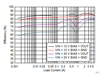
| VOUT = 5 V | fSW = 2200 kHz | Auto Mode |
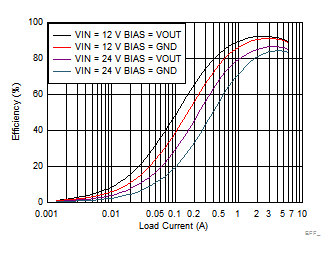
| VOUT = 5 V | fSW = 2200 kHz | FPWM Mode |
TI recommends tying the BIAS pin to VOUT when VOUT is equal to or greater than 3.3 V and no greater than 18 V. Tie the BIAS pin to ground when not in use. A ceramic capacitor, CBIAS, can be used from the BIAS pin to ground for bypassing. If VOUT has high frequency noise or spikes during transients or fault conditions, a resistor (1 to 10 Ω) connected between VOUT to BIAS can be used together with CBIAS for filtering.
The VCC voltage is typically 3.27 V. When the LM73605/6 is operating in PFM mode with frequency foldback, VCC voltage is reduced to 3.1 V (typical) to further decrease the quiescent current and improve efficiency at very light loads. Figure 17 shows an example of VCC voltage change with mode change.
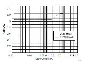
| VOUT = 5 V | fSW = 500 kHz | VIN = 12 V |
VCC voltage has an internal undervoltage lockout threshold, VCC_UVLO. When VCC voltage is higher than VCC_UVLO rising threshold, the device is active and in normal operation if VEN > VEN_VOUT_H. If VCC voltage droops below VCC_UVLO falling threshold, the VOUT is shut down.
7.3.7 Soft Start and Voltage Tracking
The LM73605/6 features controlled output voltage ramp during start-up. The soft-start feature reduces inrush current during start-up and improves system performance and reliability.
If the SS/TRK pin is floating, the LM73605/6 starts up following the fixed internal soft-start ramp.
If longer soft-start time is desired, an external capacitor can be added from SS/TRK pin to ground. There is a 2-µA (typical) internal current source, ISSC, to charge the external capacitor. For a desired soft-start time tSS, capacitance of CSS can be found by Equation 12.
where
- CSS = soft-start capacitor value (F)
- ISSC = soft-start charging current (A)
- tSS = desired soft-start time (s)
The FB voltage always follows the lower potential of the internal voltage ramp or the voltage on the SS/TRK pin. Thus, the soft-start time can only be extended longer than the internal soft-start time by connecting CSS. Use CSS to extend soft-start time when there are a large amount of output capacitors, or the output voltage is high, or the output is heavily loaded during start-up.
LM73605/6 is operating in diode emulation mode during start-up regardless of mode setting. The device is capable of starting up into pre-biased output conditions. During start-up, the device sets the minimum inductor current to zero to avoid back charging the input capacitors.
LM73605/6 can track an external voltage ramp applied to the SS/TRK pin, if the ramp is slower than the internal soft-start ramp. The external ramp final voltage after start-up must be greater than 1.5 V to avoid noise interfering with the reference voltage. Figure 18 shows how to use resistor divider to set VOUT to follow an external ramp.
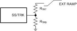 Figure 18. Soft Start Tracking External Ramp
VOUT tracking also provides the option of ramping up faster than the internal start-up ramp. The FB voltage always follows the lower potential of the internal voltage ramp and the voltage on the SS/TRK pin. Figure 19 shows the case when VOUT ramps slower than the internal ramp, while Figure 20 shows when VOUT ramps faster than the internal ramp. If the tracking ramp is delayed after the internal ramp is completed, VFB follows the tracking ramp even if it is faster than the internal ramp. Faster start-up time may result in large inductor current during start-up. Use with special care.
The SS/TRK pin is discharged to ground by an internal pulldown resistor RSSD when the output voltage is shutting down, such as in the event of UVLO, thermal shutdown, hiccup, or VEN = 0. If a large CSS is used, and the time when VEN = 0 V is very short, the CSS may not be fully discharged before the next soft start. Under this condition, the FB voltage follows the internal ramp slew rate until the voltage on CSS is reached, then follow the slew rate defined by CSS.
7.3.8 Adjustable Switching Frequency
The internal oscillator frequency is controlled by the impedance on the RT pin. If the RT pin is open circuit, the LM73605/6 operates at its default switching frequency, 500 kHz. The RT pin is not designed to be connected directly to ground. To program the switching frequency by RT resistor, Equation 13, or Figure 21, or Table 1 can be used to find the resistance value.

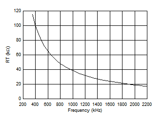 Figure 21. RT Resistance vs Switching Frequency
Table 1. Typical Frequency Setting Resistance
| SWITCHING FREQUENCY fSW (kHz) | RT RESISTANCE (kΩ) |
| 350 | 115 |
| 400 | 100 |
| 500 | 78.7 (or open) |
| 750 | 52.3 |
| 1000 | 39.2 |
| 1500 | 26.1 |
| 2000 | 19.1 |
| 2200 | 17.4 |
The choice of switching frequency is usually a compromise between conversion efficiency and the size of the solution. Lower switching frequency has lower switching losses (including gate charge losses, switch transition losses, etc.). It usually results in higher overall efficiency. However, higher switching frequency allows the use of smaller power inductor and output capacitors, hence a more compact design. Lower inductance also helps transient response (higher large signal slew rate of inductor current), and has lower DCR. The optimal switching frequency is usually a trade-off in a given application and thus needs to be determined on a case-by-case basis. Factors that need to be taken into account include input voltage range, output voltage, most frequent load current level(s), external component choices, solution size/cost requirements, efficiency and thermal management requirements.
The choice of switching frequency may also be limited whether an operating condition triggers tON_MIN or tOFF-MIN. Minimum on-time, tON-MIN, is the smallest time that the HS switch can be on. Minimum OFF-time, tOFF-MIN, is the smallest duration that the HS switch can be off.
In CCM operation, tON-MIN and tOFF_MIN limits the voltage conversion range given a selected switching frequency, FSW. The minimum duty cycle allowed is:
The maximum duty cycle allowed is:
Given an output voltage, the choice of the switching frequency affects the allowed input voltage range, solution size and efficiency. The maximum operational supply voltage can be found by:
At lower supply voltage, the switching frequency decreases once tOFF-MIN is tripped. The minimum VIN without frequency foldback can be approximated by:
With a desired VOUT, the range of allowed VIN is narrower with higher switching frequency.
LM73605/6 has an advanced frequency fold-back algorithm under both tON_MIN and tOFF_MIN conditions. With frequency foldback, stable output voltage regulation is extended to wider range of supply voltages.
At very high VIN conditions, where tON_MIN limitation is met, the switching frequency reduces to allow higher VIN while maintaining VOUT regulation. Note that the peak to peak inductor current ripple will increase with higher VIN and lower frequency. TI does not recommend designing the circuit to operate with tON_MIN under typical conditions.
At very low VIN conditions, where tOFF_MIN limitation is met, the switching frequency decreases until tON_MAX condition is met. Such frequency fold-back mechanism allows the LM73605/6 to have very low dropout voltage regardless of frequency setting.
7.3.9 Frequency Synchronization and Mode Setting
The LM73605/6 switching action can synchronize to an external clock from 350 kHz to 2.2 MHz. TI recommends connecting the external clock to the SYNC/MODE pin with an appropriate termination resistor. Ground the SYNC/MODE pin if not used.
 Figure 22. Frequency Synchronization
Recommendations for the external clock include a high level no lower than 2 V, low level no higher than 0.4 V, duty cycle between 10% and 90%, and both positive and negative pulse width no shorter than 80 ns. When the external clock fails at logic high or low, the LM73605/6 switches at the frequency programmed by the RT resistor after a time-out period. TI recommends connecting a resistor to the RT pin such that the internal oscillator frequency is the same as the external clock frequency. This allows the regulator to continue operating at approximately the same switching frequency if the external clock fails with the same control loop behavior.
The SYNC/MODE pin is also used as an operation mode control input.
- To set the operation in auto mode, connect SYNC/MODE pin to ground, or a logic signal lower than 0.3 V.
- To set the operation in FPWM mode, connect SYNC/MODE pin to a bias voltage or logic signal greater than 0.6 V.
- When the LM73605/6 is synchronized to an external clock, the operation mode is FPWM.
Table 2. SYNC/MODE Pin Settings and Operation Modes
| SYNC/MODE INPUT | SWITCHING FREQUENCY | OPERATING MODE | LIGHT LOAD BEHAVIOR |
| Logic low | Set by RT resistor | Auto mode |
|
| Logic high | Set by RT resistor | FPWM mode |
|
| External clock | Set by external clock |
7.3.10 Internal Compensation and CFF
The LM73605/6 is internally compensated. The internal compensation is designed such that the loop response is stable over a wide operating frequency and output voltage range. The internal R-C values are 500 kΩ and 30 pF respectively.
When large resistance value (MΩ) is used for RFBT, the pole formed by an internal parasitic capacitor and RFBT can be low enough to reduce the phase margin. If only low ESR output capacitors (ceramic types) are used for COUT, the control loop could have low phase margin. To provide a phase boost an external feed-forward capacitor (CFF) can be added in parallel with RFBT. Choose the CFF capacitor to provide most phase boost at the estimated crossover frequency fX:

where
- K = 20.27 with LM73605
- K = 24.16 with LM73606
Select COUT so that the fX is no higher than 1/6 of the switching frequency. Typically, fX / fSW = 1/10 to 1/8 provides a good combination of stability and performance.
Place the external feed-forward capacitor in parallel with the top resistor divider RFBT when additional phase boost is needed.
 Figure 23. Feed-Forward Capacitor for Loop Compensation
The feed-forward capacitor CFF in parallel with RFBT places an additional zero before the crossover frequency of the control loop to boost phase margin. The zero frequency can be found by Equation 19:
An additional pole is also introduced with CFF at the frequency of:
Select the CFF so that the bandwidth of the control loop without the CFF is centered between fZ-CFF and fP-CFF. The zero at fZ-CFF adds phase boost at the crossover frequency and improves transient response. The pole at fP-CFF helps maintaining proper gain margin at frequency beyond the crossover.
The need of CFF depends on RFBT and COUT. Typically, choose RFBT ≤ 100 kΩ. CFF may not be required, because the internal parasitic pole is at higher frequency. If COUT has larger ESR, and ESR zero fZ-ESR = 1 / (2π × ESR × COUT) is low enough to provide phase boost around the crossover frequency, do not use CFF. Equation 21 was tested for ceramic output capacitors:

The CFF creates a time constant with RFBT that couples in the attenuated output voltage ripple to the FB node. If the CFF value is too large, it can couple too much ripple to the FB and affect VOUT regulation. It could also couple too much transient voltage deviation and falsely trigger PGOOD flag.
7.3.11 Bootstrap Capacitor and VBOOT-UVLO
The driver of the HS switch requires a bias voltage higher than the VIN voltage. The capacitor, CBOOT in 简化原理图, connected between CBOOT and SW pins works as a charge pump to boost voltage on the CBOOT pin to (VSW + VCC). A boot diode is integrated on the die to minimize external component count. TI recommends a high-quality 0.47-µF, 6.3-V or higher voltage ceramic capacitor for CBOOT. The VBOOT_UVLO threshold is designed to maintain proper HS switch operation. If the CBOOT is not charged above this voltage with respect to SW, the device initiates a charging sequence using the LS switch before turning on the HS switch.
7.3.12 Power-Good and Overvoltage Protection
The LM73605/6 has a built-in power-good (PGOOD) flag to indicate whether the output voltage is at an appropriate level or not. The PGOOD flag can be used for start-up sequencing of multiple rails. The PGOOD pin is an open-drain output that requires a pullup resistor to an appropriate logic voltage (any voltage below 15 V). The pin can sink 5 mA of current and maintain its specified logic low level. A typical pullup resistor value is 10 kΩ to 100 kΩ. When the FB voltage is higher than VPGOOD-OV or lower than VPGOOD-UV threshold, the PGOOD internal switch is turned on, and the PGOOD pin voltage is pulled low. When the FB is within the range, the PGOOD switch is turned off, and the pin is pulled up to the voltage connected to the pullup resistor. The PGOOD function also have a deglitch timer for about 140 µs for each transition. If it is desired to pull up PGOOD pin to a voltage higher than 15 V, a resistor divider can be used to divide the voltage down.
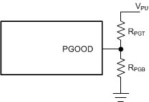 Figure 24. Divider for PGOOD Pullup Voltage
With a given pullup voltage VPU, select a desired voltage on the PGOOD pin, VPG. With a selected RPGT, the RPGB can be found by:

When the device is disabled, the output voltage is low, and the PGOOD flag indicates logic low as long as VIN > 2 V.
7.3.13 Overcurrent and Short-Circuit Protection
The LM73605/6 is protected from overcurrent conditions with cycle-by-cycle current limiting on both HS and LS MOSFETs.
The HS switch is turned off when HS current goes beyond the peak current limit, IHS-LIMIT. The LS switch can only be turned off when LS current is below LS current limit, ILS-LIMIT. If the LS switch current is higher than ILS-LIMIT at the end of a switching cycle, the switching cycle is extended until the LS current reduces below the limit.
Current limiting on both HS and LS switches provides tighter control of the maximum DC inductor current, or output current. They also help prevent runaway current at extreme conditions. With LM73605/6, the maximum output current is always limited at
The LM73605/6 employs hiccup current protection at extreme overload conditions, including short-circuit condition. Hiccup is only activated when VOUT droops below 40% (typical) of the regulation voltage and stays below for 128 consecutive switching cycles. Under overcurrent conditions when VOUT has not fallen below 40% of regulation, the LM73605/6 continues operation with cycle-by-cycle HS and LS current limiting.
Hiccup is disabled during soft-start. When hiccup is triggered, the device turns off VOUT regulation and re-tries soft start after a re-try delay time, TOC = 46 ms (typical). The long wait time allows the device, and the load, to cool down under such fault conditions. If the fault condition still exists when re-try, hiccup shuts down the device and repeats the wait and re-try cycle. If the fault condition has been removed, the device starts up normally.
If tracking was used for initial sequencing, the device restarts using the internal soft-start ramp. Hiccup mode helps to reduce the device power dissipation and die temperature under severe overcurrent conditions and short circuits. It improves system reliability and prolongs the life span of the device.
In FPWM mode, negative current protection is implemented to protect the switches from extreme negative currents. When LS switch current reaches INEG-LIMIT, LS switch turns off, and HS switch turns on to conduct the negative current. HS switch is turned off once its current reaches 0 A.
7.3.14 Thermal Shutdown
Thermal shutdown protection prevents the device from extreme junction temperature. The device is turned off when the junction temperature exceeds 160°C (typical). After thermal shutdown occurs, hysteresis prevents the device from switching until the junction temperature drops to approximately 135°C. When the junction temperature falls below 135°C, the LM73605/6 restarts.
7.4 Device Functional Modes
7.4.1 Shutdown Mode
The EN pin provides electrical on/off control of the device. When the EN pin voltage is below VEN_VCC_L, the device is in shutdown mode. The LDO output voltage VCC = 0 V and the output voltage VOUT = 0 V. In shutdown mode the quiescent current drops to a very low value.
7.4.2 Standby Mode
The internal LDO has a lower EN threshold than that required to start the regulator. When the EN pin voltage is above VEN_VCC_H, the internal LDO regulates the VCC voltage. The precision enable circuitry is turned on once VCC is above VCC_UVLO. The device is in standby mode if EN voltage is below VEN_VOUT_H. The internal MOSFETs remains in tri-state unless the voltage on EN pin goes beyond VEN_VOUT_H threshold. The LM73605/6 also employs UVLO protection. If the VCC voltage is below the VCC_UVLO level, the output of the regulator is turned off.
7.4.3 Active Mode
The LM73605/6 is in active mode when the EN voltage is above VEN_VOUT_H, and VCC is above VCC_UVLO. The simplest way to enable the operation of the LM73605/6 is to pull up the EN pin to PVIN, which allows self-start-up when the input voltage ramps up.
In active mode, depending on the load current and mode setting, the LM73605/6 is in one of four modes:
- CCM with fixed switching frequency when load current is above half of the peak-to-peak inductor current ripple;
- DCM with fixed switching frequency when load current is lower than half of the peak-to-peak inductor current ripple in CCM operation;
- PFM when switching frequency is decreased at very light load;
- Under overcurrent or overtemperature conditions, the device operates in one of the fault protection modes.
See Table 2 for mode-setting details.
7.4.3.1 CCM Mode
In CCM operation, inductor current has a continuous triangular waveform. The HS switch is on at the beginning of a switching cycle and the LS switch is turned off the end of each switching cycle. In auto mode, the LM73605/6 operates in CCM when the load current is higher than ½ of the peak-to-peak inductor current (ILripple). In FPWM mode, the LM73605/6 operates in CCM regardless of load.
In CCM operation, the switching frequency is typically constant, unless tON-MIN, tOFF-MIN, or IPEAK-MIN conditions are met. The constant switching frequency is determined by RT pin setting, or the external synchronization clock frequency. The duty cycle is also constant in CCM: D = VOUT / VIN if loss is ignored, regardless of load. The peak-to-peak inductor ripple is constant with the same VIN and VOUT, regardless of load.
With very high or very low supply voltages, when the tON-MIN or tOFF-MIN condition is met, the frequency reduces to maintain VOUT regulation with even higher or lower VIN, respectively. When the IPEAK_MIN condition is met in auto mode, switching frequency will fold back to provide higher efficiency. IPEAK_MIN is disabled in FPWM mode.
7.4.3.2 DCM Mode
DCM operation only happens in auto mode, when the load current is lower than half of the CCM inductor current ripple, and peak current is higher than IPEAK-MIN. There is no DCM in FPWM mode. DCM is also known as diode emulation mode. The LS FET is turned off when the inductor current ramps to 0 A. DCM has the same switching frequency as CCM, which is set by the RT pin. Duty cycle and peak current reduces with lighter load in DCM. DCM is more efficient than FPWM under the same condition, because of lower switching losses and lower conduction losses. When the peak current reduces to IPEAK_MIN at lighter load, the LM73605/6 operates in PFM mode.
7.4.3.3 PFM Mode
Pulse-frequency-modulation (PFM) mode is activated when peak current is lower than IPEAK-MIN, only in auto mode. Peak current is kept constant and VOUT is regulated by frequency. Efficiency is greatly improved by lowered switching losses, especially at very light loads.
In PFM operation, a small DC positive offset appears on VOUT. The lower the frequency is folded back in PFM, the more the DC offset is on VOUT. See VOUT regulation curves in Application Curves. If the DC offset on VOUT is not acceptable, a dummy load at VOUT, or lower RFBT and RFBB resistance values can be used to reduce the offset. Alternatively the device can be run in FPWM mode where the switching frequency is constant, and no offset is added to affect the VOUT accuracy unless tON_MIN is reached.
7.4.3.4 Fault Protection Mode
The LM73605/6 has hiccup current protection at extreme overload and short circuit conditions. Hiccup is activated when VOUT droops below 40% (typical) of the regulation voltage and stays for 128 consecutive switching cycles. Hiccup is disabled during soft start. In hiccup, the device turns off VOUT and re-tries soft start after 46-ms wait time. Cycle repeats until overcurrent fault condition has been removed. Hiccup mode helps to reduce the device power dissipation and die temperature under severe overcurrent conditions and short circuits. It improves system reliability and prolongs the life span of the device.
Under overcurrent conditions when VOUT droops below regulation but above 40% of regulated voltage, the LM73605/6 stays in cycle-by-cycle HS and LS current limiting protection mode.
Thermal shutdown prevents the device from extreme junction temperature by turning off the device when the junction temperature exceeds 160°C (typical). After thermal shutdown occurs, hysteresis prevents the device from switching until the junction temperature drops to approximately 135°C. When the junction temperature falls below 135°C, the LM73605/6 restarts.