ZHCSH36 September 2017 LM73605 , LM73606
PRODUCTION DATA.
- 1 特性
- 2 应用
- 3 说明
- 4 修订历史记录
- 5 Pin Configuration and Functions
- 6 Specifications
-
7 Detailed Description
- 7.1 Overview
- 7.2 Functional Block Diagram
- 7.3
Feature Description
- 7.3.1 Synchronous Step-Down Regulator
- 7.3.2 Auto Mode and FPWM Mode
- 7.3.3 Fixed-Frequency Peak Current-Mode Control
- 7.3.4 Adjustable Output Voltage
- 7.3.5 Enable and UVLO
- 7.3.6 Internal LDO, VCC_UVLO, and BIAS Input
- 7.3.7 Soft Start and Voltage Tracking
- 7.3.8 Adjustable Switching Frequency
- 7.3.9 Frequency Synchronization and Mode Setting
- 7.3.10 Internal Compensation and CFF
- 7.3.11 Bootstrap Capacitor and VBOOT-UVLO
- 7.3.12 Power-Good and Overvoltage Protection
- 7.3.13 Overcurrent and Short-Circuit Protection
- 7.3.14 Thermal Shutdown
- 7.4 Device Functional Modes
-
8 Application and Implementation
- 8.1 Application Information
- 8.2
Typical Application
- 8.2.1 Design Requirements
- 8.2.2
Detailed Design Procedure
- 8.2.2.1 Custom Design With WEBENCH® Tools
- 8.2.2.2 Output Voltage Setpoint
- 8.2.2.3 Switching Frequency
- 8.2.2.4 Input Capacitors
- 8.2.2.5 Inductor Selection
- 8.2.2.6 Output Capacitor Selection
- 8.2.2.7 Feed-Forward Capacitor
- 8.2.2.8 Bootstrap Capacitors
- 8.2.2.9 VCC Capacitor
- 8.2.2.10 BIAS
- 8.2.2.11 Soft Start
- 8.2.2.12 Undervoltage Lockout Setpoint
- 8.2.2.13 PGOOD
- 8.2.3 Application Curves
- 9 Power Supply Recommendations
- 10Layout
- 11器件和文档支持
- 12机械、封装和可订购信息
10 Layout
10.1 Layout Guidelines
The performance of any switching converter depends heavily upon the layout of the PCB. Use the following guidelines to design a PCB layout with optimum power conversion performance, EMI performance, and thermal performance.
- Place ceramic high frequency bypass capacitors as close as possible to the PVIN and PGND pins, which are right next to each other on the package. Place the small value ceramic capacitor closest to the pins. This is very important for EMI performance.
- Use short and wide traces, or localized IC layer planes, for high current paths, such as VIN, VOUT, SW and GND connections. Short and wide copper traces reduce power loss and noise due to low parasitic resistance and inductance. Wide copper traces also help reduce die temperature, because they also provide wide heat dissipation paths. Use thick copper (2 oz) on high current layer(s) if possible.
- Confine pulsing current paths (VIN, SW, and ground return for VIN) on the device layer as much as possible to prevent switching noises from contaminating other layers.
- CBOOT capacitor also contains pulsing current. Place CBOOT close to the pin and route to SW with short trace. The pinout of the device makes it easy to optimize the CBOOT placement and routing.
- Use a solid ground plane at the layer right underneath the device as a noise shielding and heat dissipation path.
- Place the VCC bypass capacitor close to the VCC pin. Tie the ground pad of the capacitor to the ground plane using a via right next to it.
- Use via next to AGND pin to the ground plane.
- Minimize trace length to the FB pin. Both feedback resistors must be located right next to the FB pin. Tie the ground side of RFBB to the ground plane with a via right next to it. Place CFF directly in parallel with RFBT if used.
- If VOUT accuracy at the load is important, make sure the VOUT sense point is made close to the load. Route VOUT sense to RFBT through a path away from noisy nodes and preferably on a layer on the other side of the ground plane. If BIAS is connected to VOUT, do not use the same trace to route VOUT to BIAS and to RFBT. BIAS current contains pulsing driver current and it changes with operating mode. Use separated traces for BIAS and VOUT sense to optimize VOUT regulation accuracy.
- Provide adequate device heat sinking. Use an array of heat-sinking vias to connect the exposed pad to the ground plane and the bottom PCB layer. Connect the DAP and NC pins on the short sides of the device to the GND net, so that IC layer ground copper can provide an optimal dog-bone shape heat sink. Heat generated on the die can flow directly from device junction to the DAP then to the copper and spread to the wider copper outside of the device. Try to keep copper area solid on the top and bottom layer around thermal vias on the DAP to optimize heat dissipation.
10.1.1 Layout For EMI Reduction
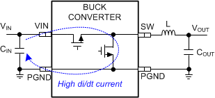
To optimize EMI performance, place the components in the high di/dt current path, as shown in Figure 75, as close as possible to each other. When the components are close to each other, the area of the loop enclosed by these components, and the parasitic inductance of this loop, are minimized. The noises generated by the pulsing current and parasitic inductances are then minimized.
 Figure 75. Pulsing Current Path of Buck Converter
In a buck converter, the high di/dt current path is composed of the HS and LS MOSFETs and the input capacitors. Because the two MOSFETs are integrated inside the device, they are closer to each other than in discrete solutions. PVIN and PGND pins are the connections from the MOSFETs to the input capacitors. The first step of the layout must be placing the input capacitors, especially the small value ceramic bypass one, as close as possible to PVIN and PGND pins.
The LM73605/6 pinout is optimized for low EMI layout. Multiple pins are used for PVIN and PGND to minimized bond wire resistances and inductances. The PVIN and PGND pins are right next to each other to simplify optimal layout. The CBOOT pin is placed next to SW pin for easy and compact CBOOT capacitor layout.
10.1.2 Ground Plane
The ground plane of a PCB provides the best return path for the pulsing current on the device layer. Make sure the ground plane is solid, especially the part right underneath the pulsing current paths. Solid copper under a pulsing current path provide a mirrored return path for the high frequency components and minimize voltage spikes generated by the pulsing current. It shields the layers on the other side of the plane from switching noises. Route signal traces on the other side of the ground plane as much as possible. Use multiple vias in parallel to connect the grounds on the device layer to the ground plane.
10.1.3 Optimize Thermal Performance
The key to thermal optimization on PCB design is to provide heat transferring paths from the device to the outer large copper area. Use thick copper (2 oz) on high current layer(s) if possible. Use thermal vias under the DAP to transfer heat to other layers. Connect NC pins to the GND net, so that GND copper can run underneath the device to create dog-bone shape heat sink. Try to leave copper solid on IC side as much as possible above and below the device. Place components and route traces away from major heat transferring paths if possible, to avoid blocking heat dissipation path. Try to leave copper solid, free of components and traces, around the thermal vias on the other side of the board as well. Solid copper behaves as heat sink to spread the heat to a larger area and provide more contact area to the air.
When calculating power dissipation, use the maximum input voltage and the average output current for the application. Many common operating conditions are provided in Application Curves. Less common applications can be derived through interpolation. In all designs, the junction temperature must be kept below the rated maximum of 125°C.
The thermal characteristics of the LM73605/6 are specified using the parameter RθJA, which characterize thermal resistance from the junction of the silicon to the ambient in a specific system. Although the value of RθJA is dependant on many variables, it still can be used to approximate the operating junction temperature of the device. To obtain an estimate of the device junction temperature, one may use Equation 30:
where
- TJ = junction temperature in °C
- PIC_LOSS = VIN × IIN × (1 − Efficiency) − 1.1 × IOUT × DCR
- DCR = inductor DC parasitic resistance in Ω
- RθJA = junction-to-ambient thermal resistance of the device in °C/W
- TA = ambient temperature in °C.
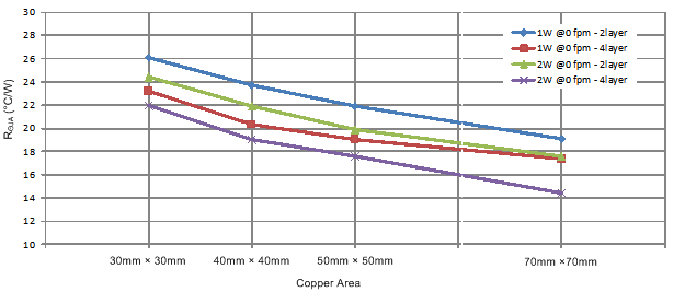
The maximum operating junction temperature of the LM73605/6 is 125°C. RθJA is highly related to PCB size and layout, as well as environmental factors such as heat sinking and air flow. Figure 76 shows measured results of RθJA with different copper area on 2-layer boards and 4-layer boards, with 1-W and 2-W power dissipation on the LM73605/6.
 Figure 76. Measured RθJA vs PCB Copper Area on 2-Layer Boards and 4-Layer Boards
10.2 Layout Example
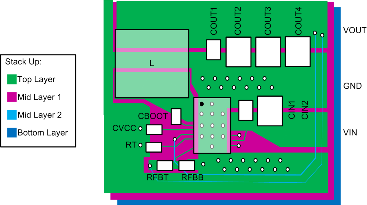
A layout example is shown in Figure 77. A four-layer board is used with 2-oz copper on the top and bottom layers and 1-oz copper on the inner two layers. Figure 77 shows the relative scale of the LM73605/6 device with 0805 and 1210 input and output capacitors, 7-mm × 7-mm inductor and 0603 case size for all other passive components. The trace width of the signal connections are not to scale.
The components are placed on the top layer and the high current paths are routed on the top layer as well. The remaining space on the top layer can be filled with GND polygon. Thermal vias are used under the DAP and around the device. The GND copper was extended to the outside of the device, which serves as copper heat sink.
The mid-layer 1 is right underneath the top layer. It is a solid ground plane, which serves as noise shielding and heat dissipation path.
The VOUT sense trace is routed on the 3rd layer, which is mid-layer 2. Ground plane provided noise shielding for the sense trace. The VOUT to BIAS connection is routed by a separate trace.
The bottom layer is also a solid ground copper in this example. Solid copper provides best heat sinking for the device. If components and traces need to be on the bottom layer, leave the area around thermal vias as solid as possible. Try not to cut heat dissipation path by a trace. The board can be used for various frequencies and output voltages, with component variation. For more details, see the LM73605/LM73606 EVM User's Guide.
 Figure 77. LM73605/6 Layout Example